STM32 MCU Basic
What is STM32
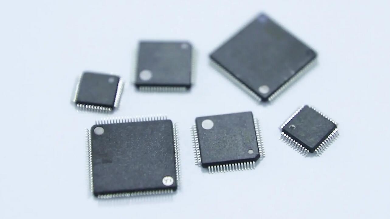
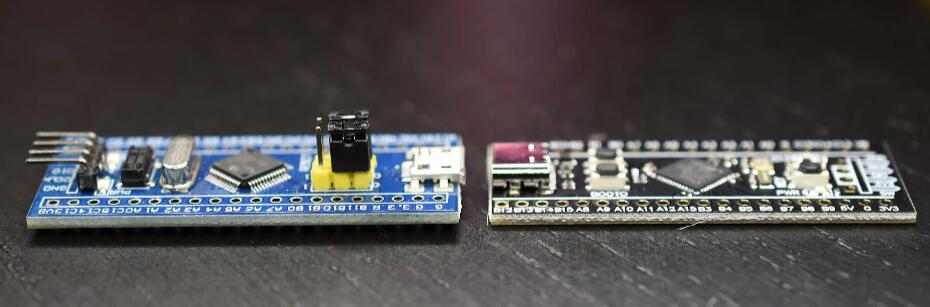
STM32, literally, ST refers to STMicroelectronics, M is the abbreviation of Micro-electronics, and 32 means 32 bits. That is, STM32 refers to the 32-bit MCU developed by ST. The base of STM32 is the 32Cortex-M3 processor with ARMv7 architecture produced by ARM.
What Can STM32 Do?
STM32 is a microcontroller with a large number of serial and parallel communication peripherals, such as USART, I2C, SPI, etc. It can connect many sensors and control many electronic components. In real life, STM32 is found in many electrical products we come into contact with, such as smart bracelets, micro aircraft, balance cars, mobile POST machines, smart rice cookers, 3D printers, smart bracelets, aircraft and etc.
STM32 Classifications
From the kernel, there are Context-M0, M3, M4, and M7. See the following table for details:
|
CPU Bits
|
Core
|
Series
|
Description
|
|
32-bit
|
Cortex-M0
|
STM32-F0
|
Beginner level
|
|
STM32-L0
|
Low power consumption
|
|
Cortex-M3
|
STM32-F1
|
Basic type, main frequency 72MHz
|
|
STM32-F2
|
High performance
|
|
STM32-L1
|
Low power consumption
|
|
Cortex-M4
|
STM32-F3
|
Mixed signal
|
|
STM32-F4
|
High performance, main frequency 180MHz
|
|
STM32-L4
|
Low power consumption
|
|
Cortex-M7
|
STM32-F7
|
High efficiency
|
|
8-bit
|
Super version 6502
|
STM8S
|
Standard series
|
|
STM8AF
|
Standard series for automotive parts
|
|
STM8AL
|
Low Power for automotive parts
|
|
STM8L
|
Low power consumption
|
Compared with F1, F4 (above 429 series) has a different core and improved main frequency. The obvious feature of the upgrade is that it has an LCD controller and camera interface, and supports SDRAM, which will be given priority in project selection.
STM32 Naming Convention
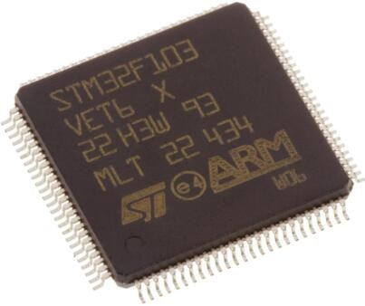
The STM32F series is a 32-bit ARM microcontroller in the middle and low end, and its core is Cortex-M3. Take STM32F103VET6 as an example:
|
-
|
STM32
|
F
|
103
|
V
|
E
|
T
|
6
|
|
Family
|
STM32 represents the 32-bit MCU
|
|
Type
|
F indicates the basic type
|
|
Function
|
Basic
|
|
Pins Number
|
V means 100pin, the commonly used are: C-48, R-64, Z-144, B-208, N-216
|
|
Flash Cap
|
E means 512kB, commonly used are: C-256, E-512, I-2048
|
|
Package
|
T stands for QFP and is the most commonly used type.
|
|
Temperature
|
6 indicates temperature class A: - 40~85 ° C
|
The more detailed naming methods are presented as follows:
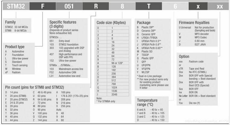
Figure 1: Naming Methods Expressions
How to Select the MCU?
Context-M3 F1 series are generally used for general applications and those that do not need to connect to a large screen. Because high performance requires a large amount of data calculation, and an external RGB large screen, choosing the Context-M4 core F429 series. After determining the general direction, the next step is the smaller parts. First determine the number of pins, more pins will have more functions, and the price will be more expensive.
After determining the number of pins, next select the Flash. MCUs with the same number of pins will have different flash to choose from, according to actual needs. If the program is large, choose a larger flash. Some products with a monthly shipment volume of millions are not only MCUs, but also resistors and capacitors that can be used as little as possible, and even the number of PCB vias must be calculated. So the selection of components in the project is very knowledgeable.
I/O Introduction
How to allocate I/O in schematics?
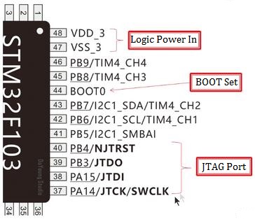
Before drawing the schematic diagram, the general practice is to classify the pins first, and then start to draw it. For pin classification, see Table 1.
Table 1: Pin Classification Descriptions
|
Pin Classification
|
Description
|
|
Power Supply
|
(VBRT),(VDD VSS),(VDDA VSSA),(VREF+ VREF-)etc.
|
|
Crystal oscillator I/O
|
Main crystal oscillator I/O, RTC crystal oscillator I/O
|
|
Download I/O
|
I/O downloaded from JTAG: JTMS JTCK JTDI JTDO NJTRST
|
|
BOOT I/O
|
BOOT0, BOOT1, Start method for location system
|
|
Reset I/O
|
NRST, for external reset
|
|
Note: The above 5 parts consists of the minimum system.
|
|
GPIO
|
Dedicated devices are connected to dedicated buses, such as I2C, SPI, SDIO, FSMC, and DCMI, all of which need to be connected to dedicated I/O
|
|
Ordinary components are connected to GPIO, such as buzzer, LED, button, etc., use ordinary GPIO
|
|
Excess can be used according to the needs of the project
|
The minimum system of STM32F103 consists of backup power supply, download interface, filter capacitor, start terminal and clock circuit. While the filter capacitor is mainly used to stabilize the voltage of the CPU power. Since there are 12 groups of CPU power, 12 100nF capacitors are used to stabilize each. When wiring, the closer each capacitor is to the power supply end, the better.
How to Find the Function of I/O?
If you want to allocate I/O according to the function, you must first know the function first, which can be found in the official data manual. When studying, there are two official materials that we often use, one is the Reference Manual and the other is the Data Sheet. The specific differences between the two are shown in Table 2.
Table 2: Differences between Reference Manual and Data Sheet
|
|
Catalog
|
Description
|
|
Reference Manual
|
Register and on-chip Peripherals
|
The function and use of each peripheral on the chip are described in detail, including registers. When programming, you need to repeatedly check.
|
|
Data Sheet
|
Function Overview
|
Introduce the main functions of the chip in general for selection.
|
|
Pin Description
|
Pin functions, schematic diagrams, need to be referenced when writing programs
|
|
Memory Map
|
Chip's memory map, bus addresses and included peripherals
|
|
Package Features
|
Chip's package, pin size, etc.
|
Table 3: Pin Definitions in the Data Sheet
|
Pins
|
Pin Name
|
Type
|
I’O level
|
Main function (after reset)
|
Alternate functions
|
|
LFBGA144
|
LFBGA100
|
WLCSP64
|
LGFP64
|
LGFP100
|
LGFP144
|
Default
|
Remap
|
|
A3
|
A3
|
-
|
-
|
1
|
1
|
PE2
|
I/O
|
FT
|
PE2
|
TRACECK/FSMC_A23
|
-
|
|
A2
|
B3
|
-
|
-
|
2
|
2
|
PE3
|
I/O
|
FT
|
PE3
|
TRACED0/FSMC_A19
|
-
|
|
B2
|
C3
|
-
|
-
|
3
|
3
|
PE4
|
I/O
|
FT
|
PE4
|
TRACED1/FSMC_A20
|
-
|
|
B3
|
D3
|
-
|
-
|
4
|
4
|
PE5
|
I/O
|
FT
|
PE5
|
TRACED2/FSMC_A21
|
-
|
|
B4
|
E3
|
-
|
-
|
5
|
5
|
PE6
|
I/O
|
FT
|
PE6
|
TRACED3/FSMC_A22
|
-
|
|
C2
|
B2
|
C6
|
I
|
6
|
6
|
VBAT
|
S
|
-
|
VBAT
|
-
|
-
|
Table 4: Interpretation of Pin Definitions
|
Name
|
Abbreviation
|
Description
|
|
Pin Number
|
Numbers indicate LQFP packages, and English letters indicate BGA packages. List 6 package models, according to the actual situation to choose.
|
|
Pin Name
|
Refers to the pin name in reset state
|
|
Pin Type
|
S
|
power pin
|
|
I
|
input pin
|
|
I/O
|
input and output pins
|
|
I/O Structure
|
FT
|
compatible with 5V
|
|
TTa
|
only supports 3V3, and directly to ADC
|
|
B
|
BOOT pin
|
|
RST
|
Reset pin, internally with weak pull-up
|
|
Main Function
|
Function after the reset of each pin
|
|
Multiplexing Function
|
This refers to the default reset function of I / O.
|
|
Remap Function
|
Except the above-mentioned functions, I/O can also be mapped to other I/O by remapping, which can increase the diversity and flexibility of I/O port functions
|
STM32F103 Interface Diagrams
Start Assigning Schematic I/O
For example, the MCU model used by our F103 guide is STM32F103VET6, and the package is LQFP100. We found the pin definition of this package in the data sheet, and then copied them one by one according to the pin number, and organized them into an excel table. The specific sorting method can be classified according to the pin classification when drawing the schematic diagram in Table 1. After the assignment, start to draw the complete schematic.
STM32F103 Series Example: STM32F103VET6
The STM32F103VET6 is a 32-bit high-density performance line Microcontroller Unit offers three 12-bit ADCs and 4 general-purpose 16-bit timers plus two PWM timers, as well as standard and advanced communication interfaces up to two I²Cs, three SPIs and two I²Ss, one SDIO, five USARTs and an USB and a CAN.
STM32F103VET6 Specifications
|
Core Architecture
|
ARM
|
|
Data Bus Width
|
32b
|
|
Density
|
4Mb
|
|
Flash Memory Size
|
512kB
|
|
Frequency
|
72MHz
|
|
Interface
|
CAN, I2C, I2S, IrDA, LIN, SDIO, SPI, UART, USART, USB
|
|
Max Operating Temperature
|
85 °C
|
|
Max Power Dissipation
|
434 mW
|
|
Max Supply Voltage
|
3.6V
|
|
Memory Size
|
512kB
|
|
Memory Type
|
FLASH
|
|
Min Operating Temperature
|
-40 °C
|
|
Min Supply Voltage
|
2V
|
|
Nominal Supply Current
|
1.9µA
|
|
Number of A/D Converters
|
3
|
|
Number of ADC Channels
|
16
|
|
Number of Bits
|
32
|
|
Number of Channels
|
16
|
|
Number of D/A Converters
|
2
|
|
Number of I2C Channels
|
2
|
|
Number of I/Os
|
80
|
|
Number of Programmable I/O
|
80
|
|
Number of PWM Channels
|
16
|
|
Number of SPI Channels
|
3
|
|
Number of Timers/Counters
|
8
|
|
Number of UART Channels
|
2
|
|
Number of USART Channels
|
3
|
|
Oscillator Type
|
Internal
|
|
Peripherals
|
DMA, I2C, POR, PWM, Temp Sensor, WDT
|
|
RAM Size
|
64kB
|
|
Termination
|
SMD/SMT
|
|
RoHS Status
|
ROHS3 Compliant
|
|
Moisture Sensitivity Level (MSL)
|
3 (168 Hours)
|
STM32F103VET6 Pinout
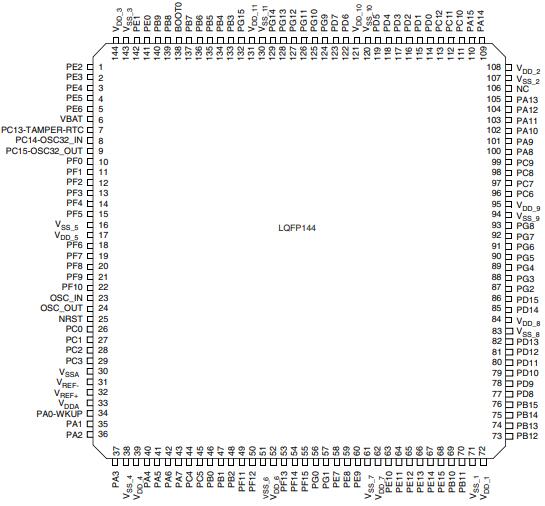
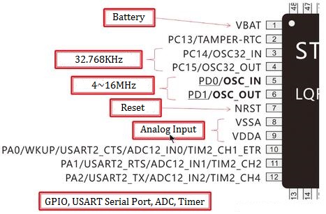
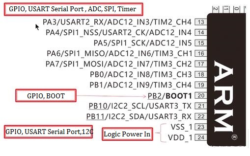
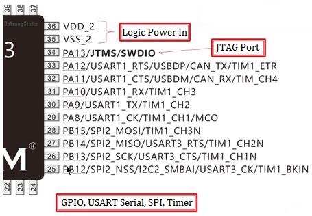
Figure 2: LQFP144 Pinout
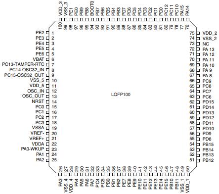
Figure 3: LQFP100 Pinout
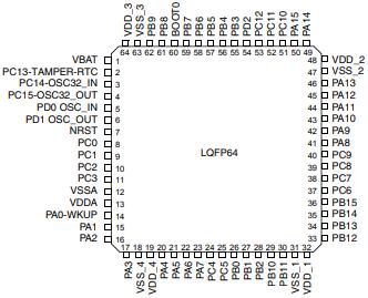
Figure 4: LQFP64 Pinout
STM32F103VE Features
1. Core: ARM® 32-bit Cortex®-M3 CPU
* 72 MHz maximum frequency, 1.25 DMIPS/MHz (Dhrystone 2.1) performance at 0 wait state memory access
* Single-cycle multiplication and hardware division
2. Memories
* 256 to 512 Kbytes of Flash memory
* up to 64 Kbytes of SRAM
* Flexible static memory controller with 4 Chip Select. Supports Compact Flash, SRAM, PSRAM, 3) NOR and NAND memories
* LCD parallel interface, 8080/6800 modes
3. NOR and NAND memories
* LCD parallel interface, 8080/6800 modes
4. Clock, reset and supply management
* 2.0 to 3.6 V application supply and I/Os
* POR, PDR, and programmable voltage detector (PVD)
* 4-to-16 MHz crystal oscillator
* Internal 8 MHz factory-trimmed RC
* Internal 40 kHz RC with calibration
* 32 kHz oscillator for RTC with calibration
5. Low power
* Sleep, Stop and Standby modes
* VBAT supply for RTC and backup registers
6. 3 × 12-bit, 1 μs A/D converters (up to 21 channels)
* Conversion range: 0 to 3.6 V
* Triple-sample and hold capability
* Temperature sensor
7. 2 × 12-bit D/A converters
8. DMA: 12-channel DMA controller
* Supported peripherals: timers, ADCs, DAC, SDIO, I2Ss, SPIs, I2Cs and USARTs
9. Debug mode
* Serial wire debug (SWD) & JTAG interfaces
* Cortex®-M3 Embedded Trace Macrocell™
10. Up to 112 fast I/O ports
* 51/80/112 I/Os, all mappable on 16 external interrupt vectors and almost all 5 V-tolerant
11. Up to 11 timers
* Up to four 16-bit timers, each with up to 4 IC/OC/PWM or pulse counter and quadrature (incremental) encoder input
* 2 × 16-bit motor control PWM timers with dead-time generation and emergency stop
* 2 × watchdog timers (Independent and Window)
* SysTick timer: a 24-bit downcounter
* 2 × 16-bit basic timers to drive the DAC
12. Up to 13 communication interfaces
* Up to 2 × I2C interfaces (SMBus/PMBus)
* Up to 5 USARTs (ISO 7816 interface, LIN, IrDA capability, modem control)
* Up to 3 SPIs (18 Mbit/s), 2 with I2S interface multiplexed
* CAN interface (2.0B Active)
* USB 2.0 full speed interface
* SDIO interface
13. CRC calculation unit, 96-bit unique ID
14. ECOPACK® packages
Applications
* Computers & Computer Peripherals
* Communications & Networking
* Industrial Applications
* PLCs
* GPS
* Alarm Systems
* Arduino IDE
* HVAC Systems
* Sensors
* Printers
* Power Inverters
* Portable Devices
* Medical Equipment
* Motor Drive & Control
* Video & Vision

 English