MCU (microcontroller) peripherals are used to help the microcontroller easy to achieve various functions. In addition to its three major components CPU, IO, and memory, there are some other things, like serial port controllers, I2C controllers, which are called peripherals. The functions of the early MCU were very single, for example, it has no interrupt function and serial communication function. When used MCUs to make products, we could only expand some special chips externally (interrupt controller chip, serial communication chips) to make a special purpose. In order to achieve different task requirements, there will be different peripherals, and they are also diverse. Here we will talk about MCU communication peripherals: UART, SPI, I2C, USB, SDIO, etc.
MCU Communication Peripherals Introduction
Next, we will explain them in detail, and at the beginning you should know the necessary theories.
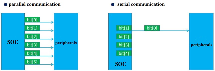
Figure 1: Communication Ways
Synchronous communication: including clocks, such as I2C bus, SPI bus, etc.
Asynchronous communication: no clock, such as UART bus, USB bus.
Parallel communication: there are multiple data lines, and one clock can transmit multiple bits, such as PCI bus and SDIO bus.
Serial communication: there is only one data line (or a pair of differential signal lines), such as I2C, SPI, USB, etc.
Universal Asynchronous Receiver-Transmitter (UART)
UART is usually used for communication between chips and external devices. The serial port mentioned in embedded generally refers to the UART port. Embedded systems often use the UART port to connect to the COM port of the host PC (or to the USB port of the host) for debugging, so that the printf function can be redirected and printed to the display screen of the host.
During the transmission process, the UART sends out the byte data bit by bit in a serial manner, and receives the data bit by bit, and then reassembles it into byte data. UART transmission rate is measured by baud rate.
UART Timing
Start bit (START): Before starting data transmission, the sender needs to send a low level '0' to indicate the beginning of the transmission character.
Data bit: After the start bit, the data can be 5, 6, 7, 8, 9 bits, forming a character, usually 8 bits.
Parity bit: Verify the correctness of data transmission, this bit can be omitted.
Stop bit: data end flag, can be 1-bit, 1.5-bit, 2-bit high level.
Serial Peripheral Interface (SPI)
SPI is a commonly used interface module in MCU. It works in a master-slave manner, usually with one master device and one or more slave devices, requiring at least 4 wires (supporting full-duplex mode) or 3 wires (supporting half-duplex mode), which are respectively SDI (data input ), SDO (data output), SCK (clock), CS (chip select).
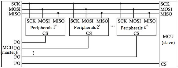
Figure 2: SPI Hardware Block Diagram
Ports:
SSN: Chip select pin, Master is responsible for sending chip select signal.
SCK: Clock pin, Master is responsible for sending clock signal.
MOSI: Master Out Slave In data line, and Master sends signal pin.
MISO: Master In Slave Out data line, and Master reads data pin.
Master read and write operations are performed synchronously, and Master sends chip select signal and clock signal. MOSI and MISO transmit data synchronously in each clock cycle.
SPI belongs to the general TTL level, and the transmission distance is generally 12 meters (often used for on-board communication, not for the device).
The maximum clock frequency of the SPI module is 1/2 of the system clock frequency. The transmission rate of SPI is mainly limited by the influence of the CPU, but when used in a very high-speed communication device, its maximum clock frequency may restrict the transmission rate.
Inter-Integrated Circuit (I2C)
I2C is a commonly used interface module in MCU. It is a simple, two-way two-wire synchronous serial bus developed by Philips. It only needs two bus lines: a serial data line SDA and a serial clock line SCL to support bidirectional communication. The main features of I2C are as follows:
1) Support as an I2C master device to write data or read data to an external I2C slave device.
2) Supports generating sending or receiving terminals.
3) Support to configure the frequency of the serial clock line SCL through the register.
4) Each device connected to the bus can be identified using a unique address.
5) For the real multi-master bus, when two or more hosts initiate data transmission at the same time, the data can be prevented from being destroyed through collision detection and arbitration.
Ports:
SCL: Clock pin, Master is responsible for sending clock signal.
SDA: Data pin, both Master and Slave can send data signals.
Master write operation: Master sends the corresponding Slave device address and data information.
Master read operation: Master sends the corresponding Slave device address, and the corresponding Slave sends data information.
All Slave devices on the I2C bus need to be configured with addresses, usually through pin configuration.
When SCL is at high level, SDA changes from high to low to become a START signal; when it is at high level, SDA changes from low to high as a STOP signal.
USB
Modern MCU families all have a USB peripheral. Standardized and integrated connectors make it easy to connect MCUs to USB cables and common drivers and application programming interfaces, or APIs, provide easy access to the data and control elements needed to transmit and receive packets of information over a USB connection. A host may have multiple host controllers, and each controller can manage up to 127 ports. USB communication uses pipes, or logical channels, that connect the host controller and device endpoints. In addition, a USB device can have up to 32 endpoints (16 inputs and 16 outputs).
USB has multiple data transfer rates (1.5 Mbit/s low speed, 12Mbit/s full speed, 480Mbit/s high speed, 5Gbit/s super speed, and 10 Gbit/s super speed+), and the host can use special enumerated process to determine the data rate for each device.
Other Supplements
Interface Mapping
Initialize the UART of the MCU, and realize the sending and receiving of USB data through the UART.
Software Setting
1) USB is set to CDC class.
void USB_CDC_Init(void)
{
//USB1.1, configure the USB as USB1.1
g_usbVer = 0;
//0:internal oscillator; 1:external oscillator
USBC_PHY_Init(0);
CCM->PHYPA |= 0x0e00; //no need to supply VBUS.
/* Global USB Register */
//gUSBC_fifoReg = (USBCFIFO_Reg*)(USBC_BASE_ADDR+0x1A);
gUSBC_fifoReg = (USBCFIFO_Reg*)(USBC_BASE_ADDR+0x60);
gUSBC_ComReg = (USBCCommonReg*)USBC_BASE_ADDR;
gUSBC_IdxReg = (USBCIndexedReg*)(USBC_BASE_ADDR+0x10);
//USB data buffer
g_databuf = USB_BUFFER_ADDR;
//The suspend mode is disable before BULK-Only tranfer start
g_suspendMode = 0;
/* Setup USB register */
//enable usb common interrupt
//0 1 2 3 4 5 6 7 (bit)
//Susp Resume Reset SOF Conn Discon SessReq VBusErr
gUSBC_ComReg->INTRUSBE = USB_INTERRUPT_RESET|USB_INTERRUPT_CONNECT|USB_INTERRUPT_DISCON|USB_INTERRUPT_SUSPEND|USB_INTERRUPT_RESUME;
//enable ep0 and ep1 tx interrupts,clear other tx interrupts
gUSBC_ComReg->INTRTXE_L = USB_INTERRUPT_EP0|(1<
gUSBC_ComReg->INTRRXE_L = (1<
//ensure ep0 control/status regesters appeare in the memory map.
gUSBC_ComReg->EINDEX = CONTROL_EP;
//Enable Soft connection
if(g_usbVer == 1)
gUSBC_ComReg->UCSR = USB_POWER_SOFT_CONN|USB_POWER_HS_ENAB;
else
gUSBC_ComReg->UCSR = USB_POWER_SOFT_CONN;
g_USBAddrFlag = 0;
g_USBNewAddr = 0;
NVIC_Init(3, 3, USBC_IRQn, 2);
}
2) Initialize the serial port as interrupt mode.
void Usb_UART_init(void)
{
UART_InitTypeDef UART_InitStruct;
UART_InitStruct.UART_BaudRate = LineCoding.bitrate;
UART_InitStruct.UART_Mode = UART_INT_MODE;
UART_InitStruct.UART_Parity = UART_PARITY_NONE;
if( LineCoding.format == 0)
{
UART_InitStruct.UART_FrameLength = UART_DATA_FRAME_LEN_10BIT;
UART_InitStruct.UART_StopBits = 1;
}
else
{
UART_InitStruct.UART_FrameLength = UART_DATA_FRAME_LEN_11BIT;
UART_InitStruct.UART_StopBits = 2;
}
UART_Init(Usb_Uart, &UART_InitStruct);
}
3) The serial port receives data and sends it to the host computer through USB. You should note that when the data interval is greater than 50 milliseconds, it defaults to two packets of data.
ret = UART_RecvByte(Usb_Uart, &temp);
if(STATUS_OK == ret)
{
uart_data_buf_[i++] = temp;
len = i ;
}
else
{
if( Tool_Tc_cnt >= 50)
{
Tool_Tc_cnt = 0 ;
if(len!= 0 )
{
usb_cdc_send(INDEX_EP1, (UINT8*)uart_data_buf_, len);
i = 0 ;
len = 0 ;
}
}
}
4) USB receives data and sends the data through UART.
void USBDev_DoCDCCmd_(void)
{
UINT16 recvLen = 0;
UINT16 len;
len = 64;
memset(cdc_ctl_buf_, 0x00, sizeof(cdc_ctl_buf_));
recvLen = usb_cdc_receive(INDEX_EP2, (UINT8 *)cdc_ctl_buf_);
if (recvLen == 0)
return;
len = recvLen;
UART_SendData(Usb_Uart, cdc_ctl_buf_,len);
}
void usb_cdc_poll_(void)
{
if( (g_uchUSBStatus & BIT1) == BIT1 ) // received a packet of data
{
g_uchUSBStatus &= ~BIT1;
USBDev_DoCDCCmd_();
}
}
The above operations can achieve the same effect as the USB_TTL chips for data transmission and reception.
Secure Digital Input and Output (SDIO)
SDIO is compatible with the previous SD card, and can be connected to SDIO interface devices, such as: Bluetooth, WIFI, camera, etc. An important difference between the SDIO and SD card specifications is the addition of the low-speed standard. Its target is to support low-speed I/O capabilities with minimal hardware overhead. In addition, low-speed cards support applications like modems, barcode scanners, and GPS receivers.
STM32 SDIO Port Features
The SDIO controller of STM32 supports multimedia cards (MMC cards), SD memory cards, SD I/O cards and CE-ATA devices.
① Compatible with version 4.2 of the multimedia card system specification. Three different data bus modes are supported: 1-bit (default), 4-bit, and 8-bit.
② Full compatible with earlier multimedia card system specification.
③ Compatible with SD memory card specification version 2.0.
④ Fully compatible with SD I/O card specification version 2.0: supports two different data bus modes: 1-bit (default) and 4-bit.
⑤ Fully support CE-ATA function (fully compatible with CE-ATA digital protocol version 1.1). The data transfer rate can reach 48MHz in 8-bit bus mode.
⑥ Data and command output enable signal, used to control the external bidirectional driver.
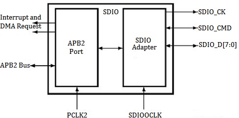
Figure 3: SDIO Block Diagram
SDIO_D0 is used for data transfer after reset. After initialization, the host can change the width of the data bus (set by ACMD6 command). If a multimedia card is connected to the bus, SDIO_D0, SDIO_D[3:0] or SDIO_D[7:0] can be used for data transfer. In addition, the protocol of MMC version V3.31 and previous versions only supports 1-bit data line, so only SDIO_D0 can be used (for the sake of versatility, as long as we detect that it is an MMC card in the program, it is set to 1-bit bus data).
SDIO Clock
Card Clock (SDIO_CK): 1-bit command or data is transmitted on the command and data lines every clock cycle. For SD or SD I/O cards, the clock frequency can vary from 0MHz to 25MHz.
SDIO adapter clock (SDIOCLK): This clock is used to drive the SDIO adapter and can be used to generate SDIO_CK clock. For F1, SDIOCLK comes from HCLK (72Mhz); for F4, it comes from PLL48CK (48Mhz).
APB2 bus interface clock (PCLK2): This clock is used to drive the APB2 bus interface of SDIO, and its frequency is PCLK2=84Mhz.
SDIO_CK calculation formula: SDIO_CK=SDIOCLK/(2+CLKDIV)
Note: SDIO_CK cannot exceed 400Khz when the SD card is initialized. After the initialization is completed, it can be set to the maximum frequency (but cannot exceed the maximum operating frequency of the SD card).
SDIO Command and Response
SDIO commands are divided into two parts: application-related commands (ACMD) and common commands (CMD). When sending ACMD, you need to send CMD55 first.
All SDIO commands and responses are transmitted on the SDIO_CMD pin, and the command length is fixed at 48 bits. The SDIO command format is shown in Table 1:
|
Bit Position
|
Width
|
Value
|
Description
|
|
47
|
1
|
0
|
Start bit
|
|
46
|
1
|
1
|
Transmit bit
|
|
[45:40]
|
6
|
-
|
Command index
|
|
[39:8]
|
32
|
-
|
Parameter
|
|
[7:1]
|
7
|
-
|
CRC7
|
|
0
|
1
|
1
|
End bit
|
Among them: except for the command index and parameters that need to be set manually, the others are controlled by the SDIO hardware automatically. The command index (such as CMD0, CMD1, etc.) is set by the SDIO_CMD register, and the command parameters are set by the SDIO_ARG register.
Generally, when the SD card receives the command line, there will be a response (except for CMD0), which we also call the response. The SDIO interface of STM32 supports 2 response types: short response (48 bits) and long response (136 bits).
The STM32 SDIO short response (48-bit) format is shown in Table 2:
|
Bit Position
|
Width
|
Value
|
Description
|
|
47
|
1
|
0
|
Start bit
|
|
46
|
1
|
0
|
Transmit bit
|
|
[45:40]
|
6
|
-
|
Command index
|
|
[39:8]
|
32
|
-
|
Parameter
|
|
[7:1]
|
7
|
-
|
CRC7 or 1111111
|
|
0
|
1
|
1
|
End bit
|
The STM32 SDIO long response (136-bit) format is shown in Table 3:
|
Bit Position
|
Width
|
Value
|
Description
|
|
135
|
1
|
0
|
Start bit
|
|
134
|
1
|
1
|
Transmit bit
|
|
[133:128]
|
6
|
111111
|
Reserve
|
|
[127:1]
|
127
|
-
|
CID or CSD,include CRC7
|
|
0
|
1
|
1
|
End bit
|
Whatever the response, the hardware will automatically filter out information such as the start bit, transmit bit, CRC7, and end bit. For a short response, the command index is stored in the SDIO_RESPCMD register, and the parameters are stored in the SDIO_RESP1 register. For the long response, only the CID/CSD bit field is reserved and stored in 4 registers such as SDIO_RESP1~SDIO_RESP4.
The SD card has a total of 6 types of responses (R1, R1b, R2, R3, R6, R7). Here we will briefly introduce R1 as an example. The R1 (ordinary response command) is a short response with a length of 48 bits, as shown in Table 4:
|
Bit Position
|
Width
|
Value
|
Description
|
|
47
|
1
|
0
|
Start bit
|
|
46
|
1
|
0
|
Transmit bit
|
|
[45:40]
|
6
|
x
|
Command index
|
|
[39:8]
|
32
|
x
|
Card status
|
|
[7:1]
|
7
|
x
|
CRC7
|
|
0
|
1
|
1
|
End bit
|
After receiving the R1 response, we can read the command index and card status information from the SDIO_RESPCMD register and SDIO_RESP1 register respectively.
SDIO Block Data Transfer
The communication between SDIO and SD card is generally transmitted in the form of data blocks, and SDIO is mostly a data block read operation.
MCU Communication Protocols
Here we will introduce TTL, RS-232, RS-422 and RS-485 in detail.
TTL (Transistor-Transistor Logic)
TTL is a serial communication commonly found in UART. Serial communication at a TTL level will always remain between the limits of 0V and Vcc, which is often 5V or 3.3V. With TTL serial, there are two unidirectional data lines. Each is driven by the sender, both high and low.
1) The hardware block diagram is as follows, TTL is used for communication between two MCUs.
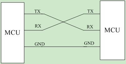
Figure 4: TTL Level Schematic Diagram
2) '0' and '1' Meaning (logic 1: 2.4V–5V, logic 0: 0V–0.5V).
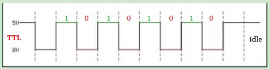
Figure 5: TTL Logic 0 and Logic 1
RS-232 (Recommended Standard 232)
RS-232 is a standard originally introduced in 1960 for serial communication transmission of data.Its signals are similar to MCU serial signals in that they transmit one bit at a time, at a specific baud rate, with or without parity and/or stop bits.
1) The hardware block diagram is as follows, TTL is used for communication between MCU and PC.
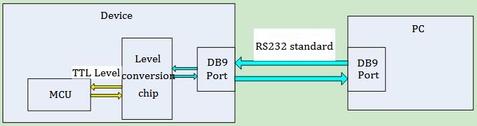
Figure 6: Schematic Diagram of RS232 Communication
2) '0' and '1' Meaning (logic 1: -15V–-3V logic 0: +3V–+15V).
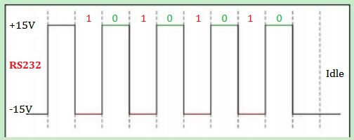
Figure 7: RS-232 Logic 1 and Logic 0
RS-422 (Recommended Standard 422)
RS-422, also known as TIA/EIA-422, is a differential standard that allows transmission over much greater distances. For example, It can provide data rates of up to 10 Mbps at distances up to 50 feet (15.24 metres). Although the RS-422 interface is similar to RS-232, it has greater distances and higher Baud rates than RS232.
Typical RS-422 is a four-wire interface. In fact, there is also a signal ground wire, a total of 5 wires. Since the receiver adopts high input impedance and the driving capability of the sending driver is stronger than that of RS-232, it is allowed to connect multiple receiving nodes on the same transmission line, up to 10 nodes. That is, one master device, and the rest are slave devices, which cannot communicate with each other, so RS-422 supports point-to-many two-way communication. The input impedance of the receiver is 4k, so the maximum load capacity of the sender is 10×4k+100Ω (termination resistance). Since the RS-422 four-wire interface uses separate sending and receiving channels, it is not necessary to control the data direction, and any necessary signal exchange between devices can be done by software or hardware to achieve.
The maximum transmission distance of RS-422 is 1219 meters, and the maximum transmission rate is 10Mb/s. The length of the balanced twisted pair is inversely proportional to the transmission rate, and the maximum distance can only be achieved when the rate is below 100kb/s. The highest data rates are only available over very short distances. Generally, the maximum transmission rate that can be obtained on a 100-meter-long twisted pair is only 1Mb/s.
Figure 8: RS422 / RS485 Pinout (DB-9)
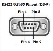
|
Pin 1
|
Pin 2
|
Pin 3
|
Pin 4
|
Pin 5
|
Pin 6
|
Pin 7
|
Pin 8
|
Pin 9
|
|
TXD-
|
TXD+
|
RTS-
|
RTS+
|
GND
|
RXD-
|
RXD+
|
CTS
|
CTS+
|
RS-485 (Recommended Standard 485)
RS-485, also known as TIA-485(-A) or EIA-485, is an industrial is a bidirectional, half-duplex standard that defines the electrical interface and physical communication of electrical devices in serial communications systems.
1) The hardware block diagram is as follows:
Note: A 120 ohm matching resistor needs to be added at the end.
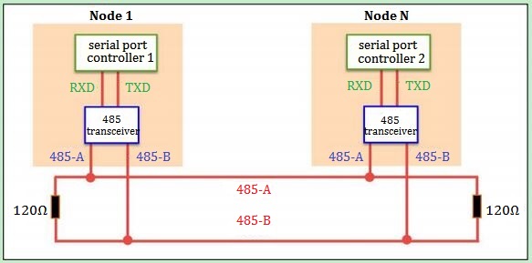
Figure 9: RS-485 Communication Network Schematic Diagram
2) '0' and '1' Meaning
The level here refers to the voltage difference between the two lines AB. Logical signals are represented by differential pressure.
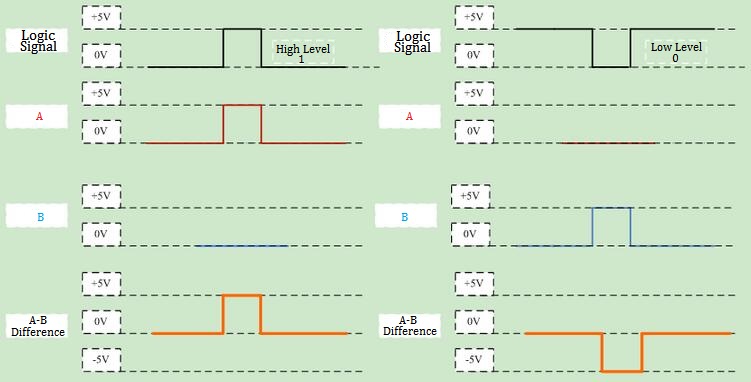
Figure 10: RS Differential Signals 1 and 0
CAN (Controller Area Network)
CAN bus is a message-based protocol, which uses two dedicated wires for communication.It allows microcontrollers and devices to communicate with each other's applications without a host computer.
Logic 1: -1.5V–0V Logic 0: +1.5V–+3V)
The level here refers to the voltage difference between CAN_High and CAN_Low.
The communication distance can reach up to 10KM (the rate is less than 5Kbps) and the rate can reach 1Mbps (the communication distance is less than 40M).
1) The hardware block diagram is as follows:
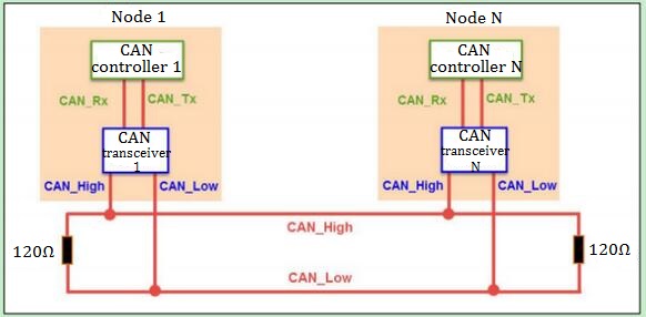
Figure 11: CAN Closed-loop Bus Communication Network
2) '0' and '1' Meaning
Signal logic represented by CAN protocol standard.
|
Signal
|
ISO11898 (High-speed)
|
ISO11519-2 (Low-speed)
|
|
Recessive (logic 1)
|
Dominant (logic 0)
|
Recessive (logic 1)
|
Dominant (logic 0)
|
|
Min
|
Typ
|
Max
|
Min
|
Typ
|
Max
|
Min
|
Typ
|
Max
|
Min
|
Typ
|
Max
|
|
CAN_High(V)
|
2.0
|
2.5
|
3.0
|
2.75
|
3.5
|
4.5
|
1.6
|
1.75
|
1.9
|
3.85
|
4.0
|
5.0
|
|
CAN_Low(V)
|
2.0
|
2.5
|
3.0
|
0.5
|
1.5
|
2.25
|
3.10
|
3.25
|
3.4
|
0
|
1.0
|
1.15
|
|
High-Low Potential Difference (V)
|
-0.5
|
0
|
0.05
|
1.5
|
2.0
|
3.0
|
-0.3
|
-1.5
|
-
|
0.3
|
3.0
|
-
|
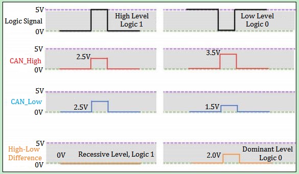
Figure 12: CAN Differential Signaling (high speed)
TTL vs RS232 vs RS422 vs RS485
|
|
TTL
|
RS232
|
RS422
|
RS485
|
|
Information Type
|
Level Signal
|
Level Signal
|
Differential Signal
|
Differential Signal
|
|
Voltage Range
|
3.3V or 5.0V
|
-15V~+15V
|
-0.25V~+6V
|
-7V~+12V
|
|
Transmission Distance
|
1m
|
10m
|
1200m
|
1200m
|
|
Transfer Mode
|
Full-duplex, Point-to-point
|
Full-duplex, Point-to-point
|
Full-duplex, Point-to-point
|
Half-duplex, Many-to-many
|
|
Transmission Rate (MAX)
|
100Kb/s
|
100Kb/s
|
10Mb/s
|
10Mb/s
|
Note:
Simplex: Only one-way communication
Half-duplex: Only one-way communication is allowed at the same time, but data cannot be accepted when sending, such as I2C.
Full-duplex: Allow two-way communication at the same time, but data cannot be accepted when sending, such as SPI, UART.
Protocol Layer
No matter which standard is used in the physical layer, as long as asynchronous transceiver is used, the data frame format of communication is the same, which consists of the following four parts: start bit, data bit, parity bit and stop bit.

Figure 13: Protocol Layer
1) Start Bit
The start signal of a data frame is represented by a logic 0 data bit.
2) Data Bit
Immediately after the start bit of the data frame is the content of the main data to be transmitted, also known as valid data, and the length of it is often agreed to be 5, 6, 7 or 8 bits long.
3) Check Digit
After the valid data, there is an optional data check digit. Since data communication is relatively more susceptible to external interference, resulting in deviations in transmitted data, a parity bit can be added to the transmission process to solve this problem. The parity method includes odd parity (odd), even parity (even), 0 parity (space), 1 parity (mark) and no parity.
Odd parity requires that the number of 1s in valid data and parity bits be odd. For example, an 8-bit long valid data is: 01101001. At this time, there are a total of 4 1s. In order to achieve the effect of odd parity, the parity bit is 1, the last transmitted data will be 8 bits of valid data plus 1 bit of parity for a total of 9 bits.
The requirements of even parity and odd parity are just the opposite. The number of 1s in the frame data and parity bits is required to be even 0.
The 0 parity means that no matter what the content in the valid data is, for example, the 0 parity is always 0, and the 1 parity is always 1.
4) Stop Bit
The stop signal of the data frame can be represented by 0.5, 1, 1.5 or 2 logic 1 data bits, as long as both parties agree.
5) Note: Communication Timing calculation
Assume a baud rate of 9600, 8 data bits, no parity, and 1 stop bit. So how long does it take to transfer 100 bytes of data?
It is known that a byte is composed of 8 bits, and only one data frame is required to transmit a byte = 1 start bit + 8 data bits + 0 parity bit + 1 stop bit = 10bit
The baud rate is 9600, that is, it takes 1/9600s to transmit one bit.
So total time = 1/9600 * 10 * 100 = 0.10417s

 English










