3D NAND is an emerging type of flash memory that solves the limitations of 2D NAND or planar flash by stacking memory particles together. In order to achieve higher storage capacity, the NAND integration process began to develop in the direction of three-dimensional stacking. Since 2018, most smartphones around the world have started to use 3D NAND flash chips. Not only smartphones, 3D NAND chips are also very popular in data centers, clouds, servers, SSDs, PCs, etc.
From 2D to 3D
Traditionally, NAND cells are arranged in a 2D structure, and the higher the number of cells, the greater the drive capacity (increased memory per chip). But as the demise of Moore's Law tells us, there's a limit to how much silicon can be shrunk. That is, the NAND flash memory with a planar structure is close to its actual expansion limit, which brings severe challenges to the semiconductor memory industry. Since there are no cells in 2D, manufacturers start stacking them one by one, which can support higher storage capacity in a smaller space, which is 3D NAND. Pairing TLC- and QLC-based SSDs with 3D stacking or V-NAND can further improve the flash performance, making the drives even more affordable.
3D NAND achieves incremental capacity by layering groups of memory cells on top of each other in a vertical stack. The more layers in a flash memory chip, the greater the total storage capacity. At present, all major manufacturers are manufacturing chips with more than 100 layers, and each has completed the development layout of flash memory with higher layers.
3D NAND Flash Development
3D TLC
Samsung, SK hynix and Kioxia / Western Digital (WD) announced information on new 3D TLC. Samsung leads the way in performance, with the lowest read latency and fastest write speeds. However, bit density is still significantly lagging, claiming a 70% jump in it this generation. Samsung was able to avoid the use of tandem stacks and could manufacture the 128-layer stack as a single layer. Competitors have all had to split the stack into two layers, increasing the number of fab steps required. Samsung's use of cascading results in a poor density. If delay this transition for another generation, this density increasing is achieved by using a combination of other technologies (most notably CMOS under array layout). In this way, Samsung is already years ahead of the competition when it comes to vertical channel aspect ratio etching, because the aspect-ratio etching of vertical channels is the most critical fabrication step for scaling 3D NAND.
The TLC flash difference between SK hynix and Kioxia/Western Digital is that SK hynix has a 512Gb chip, while Kioxia is 1Tb. Both designs have similar performance and density, despite Kioxia's touted higher speed NAND interface. Kioxia and WD announced 162-layer 3D NAND, and the layers is less than SK hynix and Micron. However, with a 10% increase in the horizontal density of the cell array, Kioxia and WD may be packing vertical channels closer together than any competitor.
In the seventh-generation 512Gb 176-layer TLC chip, Samsung began to adopt the COP (Cell-on-Periphery) structure, and the subsequent 1Tb 238L TLC product will be the second-generation COP TCAT V8 V-NAND. The memory cell array area of the COP structure is located above the peripheral devices, but some peripheral devices of the COP structure are still located outside the cells, which means that the cell array and the peripheral area below and beside the cell array must be reduced for smaller size.
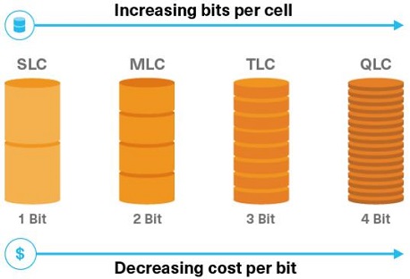
Figure 1: Storage Solutions from KIOXIA
3D QLC
The only company with a QLC update is Intel. Overall, Intel is focusing more on QLC NAND than any other competitor. This 144L QLC is the first generation of 3D NAND that Intel didn't co-develop with Micron. Intel sell its 3D NAND flash business to SK hynix with U.S $9 bln. Intel has better performance and density than QLC at tier 9X - but the QLC version of the new TLC described by SK hynix and Kioxia should be superior. Intel has given up on using 96-layer QLC to describe the block size, and the 48MB block size of 144-layer NAND also looks large.
In November 2018, starting from the fourth generation of 96-layer 3D NAND, SK hynix launched a new nomenclature - 4D PUC (Periphery Under Cell), PUC is a technology that relocates peripheral circuits to the bottom of the battery, as follows as shown in the figure. It's the trade name for a variant of the 3D architecture, and the first so-called 4D NAND devices boosted the peripheral circuitry beneath the CTF (charge-trapping flash) NAND array, saving more space on the chip and further reducing production costs.
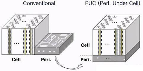
Figure 2: 4D PUC (Periphery Under Cell)
After 98 layers, SK hynix successively developed 128-layer and 176-layer 3D NAND. In August 2022, SK hynix announced that it has developed the world's highest 238-layer 4D NAND flash memory, which is also the smallest NAND, and is expected to start mass production in the first half of 2023. Now SK hynix's current 4D NAND technology is recognized as the industry standard.
The PUC architecture enables 4D NAND to allow high density in a fixed area, reducing chip size, but the disadvantage is that the stacking technology may reach its limit in the future. SK Hynix plans to overcome this obstacle with a multi-site battery (MSC) at its core, by dividing the existing battery into two smaller batteries to store data through microfabrication, reducing the number of battery stacks, and expanding battery density horizontally. It is also one of the key elements of the technical concept of SK Hynix 4D 2.0.
BiCS
KIOXIA proposed the concept of BiCS FLASH™ "batch processing technology" at an academic conference in 2007. In a BiCS FLASH™ cell, electrons are exchanged between an electrode (gray structure) passing through the center of the pillar and the charge storage film (pink). In this way, the memory cells are not stacked layer by layer, but the plate-shaped electrodes are stacked first, and then a hole is opened between them to connect the electrodes, so that the memory cells of all layers are formed at one time to reduce the manufacturing cost.
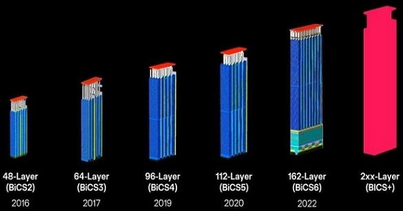
Figure 3: The Layer Development of BiCS Flash
In 2015, Kioxia & Western Digital launched 48-layer BiCS 3D NAND, 64-layer in 2017, 96-layer in 2018, and 112-layer in 2020. In 2021, Kioxia and WD announced their sixth-generation BiCS 3D NAND technology with 162 layers, which is also the first product using the CuA concept. In addition, WD said that the next generation of "BiCS+" will be launched by the end of 2023, and the number of layers should increase to more than 200.
CuA (CMOS-under-array)
Micron has used this method of building its 3D NAND array on the peripheral logic of the chip since the first generation of 32-layer 3D NAND, which is called CuA (CMOS-under-array). Place most of the NAND chip's peripheral circuitry (page buffers, sense amplifiers, charge pumps, etc.) under the vertical stack of memory cells, not side by side. A large amount of die space is saved, and more than 90% of the die area is used for the memory cell array. The architecture provides a sustainable approach for capacity growth, density, performance and cost improvements. SK hynix followed closely, called "Periphery under Cell" (PuC). Kioxia and WD demonstrated a 128-layer CuA design at ISSCC 2019, and the fifth-generation BiCS 3D NAND was finally put into production with 112 layers without CuA. And the sixth generation of BiCS 3D NAND will be a 162-layer CuA design.
In addition to saving die space, the CuA/PuC design of 3D NAND also allows the die to contain more peripheral circuits, which is more cost-effective. Divide the die's memory array into more independent planes, each with a copy of most of the peripheral circuitry. Later most 3D NAND adopting the standard is four planes per die. This provides additional parallelism, increasing performance per die, and offsets the overall performance degradation of SSDs that typically results from using fewer dies to achieve the same overall capacity.
The CuA structure is not without challenges and drawbacks. When manufacturers first switched to CuA, the successive increase in the number of layers in each generation means that there is less die space to manage the same number of memory cells, and the peripheral circuits must still be reduced. Placing peripheral circuitry beneath the memory cell array also creates new constraints. For example, Samsung mentions that this presents challenges in constructing large capacitors for charge pumps when they are no longer able to use tall metal structures that are easily included in 3D NAND stacks.
In late July 2022, Micron announced its 232-layer 3D NAND. According to Micron, this 232-layer flash achieves the highest TLC density per square millimeter (14.6 Gb/mm2). Plane density is 35% to 100% higher than similar TLC products. Because the 3D NAND device is divided into six planes (many NAND devices on the market today have only two, and some cutting-edge designs use four plane partitions to channel command and data flow) to achieve higher parallelism, thereby improving performance. On a per-chip basis, the increased parallelism improves read and write performance for both sequential and random access by enabling more read and write commands to be issued to the NAND device simultaneously. Just like a highway, the more lanes there are, the less congestion there is and the greater the flow of traffic through a given area. At present, Micron's 232-layer NAND has been mass produced.
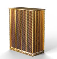
Figure 4: 232-layer 3D NAND
On-Die Parallelism:A Die with Four Planes
Dividing a NAND flash die into four planes allows the die to handle more operations in parallel, but it doesn't make it behave like four separate dies. Because parallel execution operations are restricted: for example, simultaneous writes still have to be done on the same word line within each plane. But manufacturers have been working to loosen some restrictions as the number of flash memory chips has increased. Over the past few years, manufacturers have introduced "independent" multi-plane reads, meaning simultaneous reads in different planes without any restrictions within each plane, which is a big win for random read.
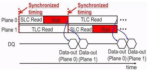
Figure 5: Synchronized Timing
Another constraint on multiplane operations is now relaxed: the timing of read operations on different planes is not required. This allows one plane to perform multiple reads from an SLC page while the other plane performs a single, slower read from a TLC or QLC page, which called asynchronous independent (multi) plane reads. The net effect is that for read operations, one large 4-plane die can now match the performance of four smaller 1-plane dies. This can alleviate the performance penalty that higher per-chip capacities impose on SSDs with only one or two chips per channel.
Kioxia and WD report that for this to work, the sharing of charge pumps between planes must be stopped to avoid untimely voltage and current fluctuations due to out-of-sync read operations. Intel also hits halfway to this capability with its 4-plane 144-layer QLC: multiple planes are paired into multiple plane groups, and each plane group can perform reads without needing to align with independent read timing.
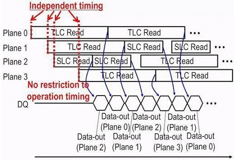
Figure 6: 144-layer QLC Timing
NAND I/O Speed
The new TLC NAND parts support I/O speeds ranging from 1.6 to 2.0 Gb/s for communication between the NAND flash die and the SSD controller. The fastest NAND SSDs run at 1.2-1.4Gb/s. NAND manufacturers can support these higher I/O speeds by ensuring that SSD controller designs will be used, likely relying on third-party controllers for SSDs. Phison's latest E18 8-lane controller for high-end PCIe 4.0 SSDs only supports 1.2Gb/s I/O speed, while the upcoming E21T 4-lane NVMe controller supports 1.6Gb/s. Silicon Motion's 8-channel SM2264 and 4-channel SM2267 support 1.6Gb/s and 1.2Gb/s I/O speeds, respectively.
Running 8 lanes at 1.2Gb/s is already enough to saturate an SSD with a PCIe 4.0 x4 connection, and the new higher I/O speeds at PCIe 5.0 aren't much use for high-end SSDs. However, more affordable 4-channel consumer SSD controllers, able to use these higher speeds to better enter the PCIe 4.0 performance realm, match or exceed the first PCIe 4.0 SSD controller (Phison E16, 8ch @ 800Mb/s ) to provide throughput. For example, the SK hynix GoldP31, advanced 4-channel controllers supports high I/O speeds on each channel, and operates with higher power efficiency than 8-channel controllers.
Achieving higher I/O speeds requires a major upgrade of the interface logic on the NAND die, as with PCI Express, and increased power consumption is a major concern. Samsung is addressing this issue by using dual-mode drivers and terminals. When higher drive strength is required due to more load on the bus (more die per channel), a PMOS transistor is used for the pullup, or an NMOS transistor can be used and the power consumption of the driver can be reduced by more than half. This gives a single interface design that works well across small consumer SSDs and large enterprise drives with more die per channel. Samsung has added individual retimer chips in multi-chip packages, which stack many NAND chips together on the same one or two channels.
3-Layer String Stacking
String stacking has been seen as a necessary means to scale 3D NAND to higher layer counts. Only Samsung can build 3D NAND with more than 100 layers at a time, and everyone else has long since switched to stacking two decks with more reasonable layer counts. That means, for example, Micron's 176-layer 3D NAND is built as 88 layers of memory cells, and then another 88 layers are built on top of that. This adds cost compared to doing all layers at once and requires careful alignment at the interface between platforms. But another option is to make the vertical channels wider to keep the aspect ratio (width to depth) within what current fab technology can etch.
Intel's 144-layer QLC design has moved to a 3-layer stack: 48+48+48 layers instead of the expected 72+72. The previous generation was a 48+48 layer design, apart from repeating the same sequence of deposition, etch and fill steps for a third time, little has changed about how the memory array manufactured. Intel affects the throughput of the fab with this approach, but it may help to better control the variation of channel and cell size from the top of the stack to the bottom, the focus on QLC and its uniqueness, this may be a bigger problem. So the decision was made to still use floating gate memory cells instead of switching to charge trap cells. If you want to know more details about it, just mark our web KUKE.

 English










