Artificial intelligence (AI) for machine learning is hot recently, such as TPU v4, GPT-4, Tongyi Qianwen and something like that. Here TPU(tensor processing units) is Google's custom-developed application-specific integrated circuits (ASIC) used to accelerate machine learning, which is an AI accelerator. It is built to optimize the TensorFlow machine learning framework, and mainly used in the AlphaGo system, as well as Google Maps, Google Photos and Google Translate, to provide applications such as search, image, voice and other models and technologies. So TPU will overlap with the GPU, but TPU is an ASIC chip and can do more, both has its own living space. Here we will talk about TPU.
Google TPU's Development
TPU v1
The TPU project started in 2014 for two reasons:
1) Computing tasks have changed: Deep neural networks have begun to emerge, and matrix multiplication and addition has become an important calculation loading.
2) CPUs and GPUs are too expensive, often costing tens of thousands of dollars. For a large data center like Google, it needs to find a cheap way to reduce TCO. So google started to develop its own chips.
David Patterson, a distinguished software engineer at Google, mentioned in his speech that TPU v1 took a total of 15 months to be made, and the cycle is relatively short. TPU v1 is mainly used for inference, regardless of training. All inferencing with the Edge TPU is executed with TensorFlow Lite libraries, and TPU v1 has a 10-fold performance advantage over the GPU.
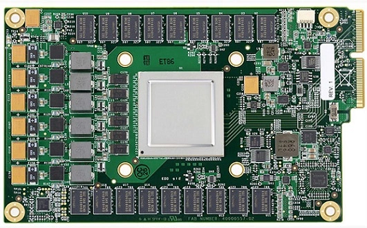
Figure 1: TPU v1 Chip
Next, look at the TPU v1 architecture diagram
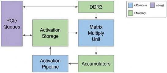
Figure 2: TPU v1 Architecture Diagram
As an accelerator, TPU v1 is connected to the Server through PCIe, and gets instructions from the Host Server, including the following 5 instructions:
1)Read_Host_Memory
2)Write_Host_Memory
3)Read_Weights
4)MatrixMultiple / Convolve
5)Activation (Sigmoid, ReLU, MaxPool....)
The characteristics of the TPU v1 chip are:
1) It is only used for inferencing, only forward, no reverse, no need to consider the support for various loss functions, the problem of storing activation for reverse use, and derivation problem, etc.
2) According to the above 5 instructions, it can be seen that the TPU only supports MatrixMultiple / Convole and specific activation functions.
3) Looking at the data path:
a) The DDR channel is responsible for the movement and data arrangement of weights/kernels, and transmits them to the MMU.
b) Activation Storage stores the output of the upper layer, and rearranges it to meet the requirements of the MMU, which serves as the input of the next layer. The first layer of the network (that is, the inference data e.g. the data picture in the split task) is also directly transmitted here through PCIe.
c) MMU systolic array
d) Accumulators do some summing operations.
e) The activation pipeline performs operations such as Relu, Sigmoid, and Pooling.
TPU v2
TPU v2 aims for training, and there are more aspects to consider than TPU v1, including the following aspects:
1) More calculations, with reverse, transpose, loss calculation, and find derivation.
2) More memory is needed to store activation, even in reverse.
3) The problem of expansion, cluster solutions are generally used to do it to speed up training.
4) The complexity of programming, TPU v1's 5 instructions can’t handle everything.
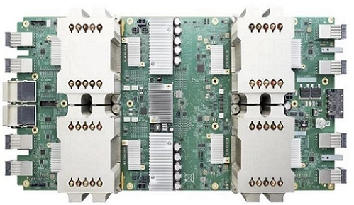
Figure 3: TPU v2 Chip
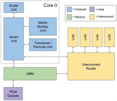
Figure 4: The TPU v2 Architecture
Compared with TPU v1, TPU v2 has the following differences:
1) Use HBM instead of DDR3, because it can provide higher bandwidth to alleviate or reduce memory bound.
2) Added interconnect, which can provide expansion capabilities (Scale Up & Scale Out). That is, two TPU Cores of a chip can exchange data efficiently (ie Scale Up), and have efficient data exchange with other TPUs through interconnect (ie Scale Out).
3) Added general purpose vector unit to replace the fixed activation function / activation pipeline.
4) There is still a Scalar Unit inside the TPU v2 core. Scalar, vector, and matrix are all available, and the versatility has become stronger. There is also transpose / permute unit, which further accelerates hardware operations such as transpose. In addition, the interconnect router has 4 links, and the bandwidth of each link is 500Gbps.
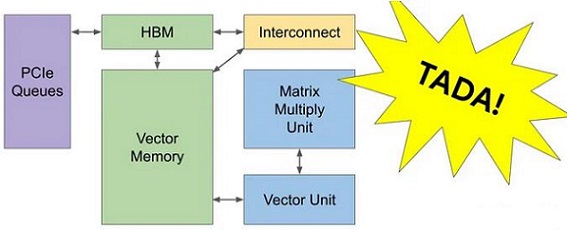
Figure 5: Differences between TPU v2 and TPU v1
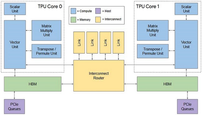
Figure 6: A Chip with TPU Cores
TPU v3
Each v3 TPU chip contains two TensorCores. Each TensorCore has two MXUs, a vector unit, and a scalar unit. The following table shows the key specifications and their values for a v3 TPU Pod. TPU v3 is further improved based on TPU v2, as shown in Figure 7:
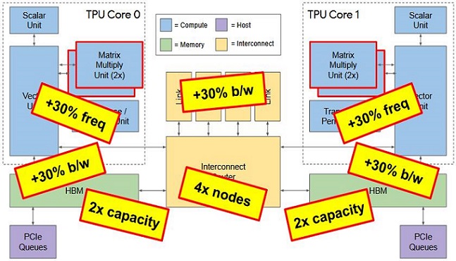
Figure 7: Differences between TPU v3 and TPU v2
Architectural details and performance characteristics of TPU v2 and v3 are available in A Domain Specific Supercomputer for Training Deep Neural Networks.
TPU v4
A TPU v4 Pod is composed of 4096 chips interconnected with reconfigurable high speed links. It has extremely high extension. For example, thousands of chips can be accelerated at the same time, so as to realize a supercomputer designed for machine learning model. In Google's design, the topology of the supercomputer is: 4x4x4 (64) TPU v4 chips are interconnected to form a cube, and then such cubs are connected together to form a total of 4096 TPUv4 super computer.
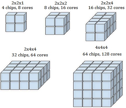
Figure 8: TPU v4 Supercomputer Topology
In such a topology, TPUv4s with close physical distances (that is, chips in the same cube) can be connected by traditional electrical interconnection (such as copper twisted wires), but TPUs that are far away (such as in cubes) must use optical interconnection. Because in such a large-scale supercomputer, the data interconnection between chips will largely determine the overall computing efficiency. For example, if the efficiency is not high enough, chips are often waiting for data from other chips to start the calculation, thus forming a waste of efficiency. In order to avoid such a situation, it is necessary to ensure chips can have high bandwidth and low latency, so optical interconnection has become the first choice for chips with long physical distances.
The use of optical interconnection in high-performance computing is not the first time, and TPU v4 is to use reconfigurable optical interconnects (optical circuit switch OCS) to quickly realize different chip interconnecting topology. It has many benefits that the topology can be changed according to specific machine learning models, and the reliability of supercomputers can be improved.
In terms of topology, the data flow requirements of different machine learning models can be roughly divided into three categories: data parallelism (each chip loads the entire model, and different chips process different data intensively), model parallelism (some layers are very large, so each chip is only responsible for a part of one layer calculation), and pipeline parallelism (different layers in the model are handed over to different chips for calculation), and different data flows correspond to different TPU topology. Because of configurable optical interconnection, the topology between TPUs can be adjusted according to the specific model data flow, so as to achieve well performance.
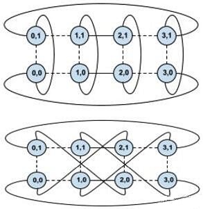
Figure 9: Fast Switching between Different Chip-to-Chip Interconnect Topologies Using Reconfigurable Optical Interconnections
Another advantage is reliability. In a supercomputer composed of such a large number of chips, there is an important factor that must be taken into account. If a small part of chips doesn’t work, how to ensure that the computer as a whole can still maintain high performance? With conventional interconnecting architectures, a single chip failure could affect the entire system. But with optical interconnection, all that needs to be done is to bypass the faulty chip, which will not affect the work of the entire system, just waste a little overall performance.
In the paper, Google gave a graph of the single-chip failure rate and the average performance impact of the system. When using configurable optical interconnects (and OCS), assuming that the chip reliability rate is 99%, the average performance improvement of overall system can be as high as 6 times without OCS.
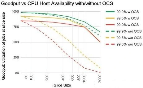
Figure 10: Goodput vs CPU Host Availability with/without OCS
To realize configurable optical interconnection, it is necessary for the optical path switch to be able to efficiently expand to an ultra-high number of interconnections (such as 1000x1000), and to achieve low switching delay, low cost, and low loss. Google believes that the existing commercial solutions are not good enough, so it has developed an OCS Palomar. The TPUv4 is using this to realize the world's first data center-level configurable optical interconnection.
Palomar uses technology based on MEMS mirror arrays. Its principle is to use a 2D MEMS mirror array to adjust the optical path by controlling the position of the mirror, so as to realize the switching of the optical path. This has the advantages of low loss, low switching delay (millisecond level) and low power consumption. Having a series of optimizations, the cost of the optical path system is also kept low, accounting for less than 5% of the cost of the entire TPUv4 supercomputer.
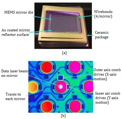
Figure 11: Palomar MEMS OCS Chip
a) Photograph of a Palomar MEMS mirror package. Inside each ceramic package is a single large die with 176 individually controllable micro-mirrors.
b) Thermal image of MEMS mirrors. Each mirror has four comb driye regions to rotate it in two directions.
Algorithm-chip Collaborative Computing Design
This design is the soul of TPU v4, including two parts, one is how to optimize the chip according to the algorithm, and the other is how to optimize the algorithm according to the chip. In the architecture of TPU v4, both are carefully considered.
Firstly analyze how TPU v4 optimizes the chip according to the algorithm. The TPU v1 in 2017 mainly solves the convolutional neural network CNN, but in 2023, the CNN acceleration has been almost solved, and now it is more about how to deal with the problem of large models. For Google, the most critical model at present is the recommendation system model that determines the company's main revenue. Therefore, the design of TPU v4 has been quite optimized for this.
In the large model of the recommendation system, the current bottleneck for acceleration is the embedding layer, which is to map high-dimensional sparse features to low-dimensional high-density features. And this can be further processed by the neural network. The implementation of the embedding layer is usually a look-up table, which can be as large as 100GB. There can be multiple such lookup tables in a recommendation system model, so that the storage capacity of the entire lookup table can reach TB level. Such a huge lookup table will make the use of distributed computing, and each embedded layer will be distributed to multiple TPU v4 chips for calculation.
For such embedding layer calculations, on the one hand, they are mainly based on 1D vector calculations, rather than 2D matrix or 3D tensor calculations; secondly, calculations are often sparse (because the input features are sparse, on the other hand, not all features will have high-density calculations and are distributed on different chips. So it is necessary to optimize shared storage to exchange data efficiently.
In order to optimize the embedding layer, a dedicated acceleration module be made in TPU v4, called Sparse Core (SC). Each SC has its own vector computing unit (scVPU), 2.5 MB local SRAM, and a memory access interface that can access up to 128TB shared HBM. In addition, SC also has some dedicated acceleration logic specially designed for embedded layer operations, including sort, reduce, concat, etc. Actually, each SC is relatively simple, so a large number of SCs are deployed in each TPU v4, but the overall area and power consumption of SCs account for only 5% of TPU v4.
In the paper, Google compared using the CPU to run the embedding layer and using the TPU v4 SC to do same thing. The results show that when running the same recommendation system, putting the embedding layer on the SC of TPU v4 can increase the running speed more than 6 times. In fact, this is also the most attractive part of domain-specific design, that is, a very large performance improvement can be obtained with a small chip area and power consumption overhead. For TPU v4, Google puts such a domain-specific design in the most critical place for the entire company, thereby leveraging very large benefits.
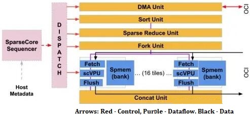
Figure 12: Sparse Core (SC) Design of TPU v4
In addition to optimizing algorithms at the chip level, TPU v4 also optimizes algorithms at the distributed computing topology level. As mentioned above, TPU v4 uses reconfigurable optical interconnection between different TPU v4 for different AI models. For this reason, Google designed a set of machine learning algorithms to determine how to configure an optical switch to improve performance. The analysis shows that for the most popular large language training models (including GPT-3 and GPT-4), the optimal TPU interconnection topology configuration found by machine learning algorithms can level the performance by 1.2-2.3 times.
Finally, Google also specially designed a neural network architecture search (NAS) algorithm for TPU v4, which can optimize artificial intelligence models according to the characteristics of TPU v4. This ensures that the optimized model can run on TPU v4 most efficiently and make full use of resources. Compared with manual optimization, the use of NAS can achieve up to 10% runtime optimization, which saves tens of millions of dollars in annual costs roughly.
Each v4 TPU chip contains two TensorCores. Each TensorCore has four MXUs, a vector unit, and a scalar unit. The following table shows the key specifications and their values for a v4 TPU Pod.
|
Key specifications
|
v4 Pod values
|
|
Peak compute per chip
|
275 teraflops (bf16 or int8)
|
|
HBM2 capacity and bandwidth
|
32 GiB, 1200 GBps
|
|
Measured min/mean/max power
|
90/170/192 W
|
|
TPU Pod size
|
4096 chips
|
|
Interconnect topology
|
3D torus
|
|
Peak compute per Pod
|
1.1 exaflops (bf16 or int8)
|
|
All-reduce bandwidth per Pod
|
1.1 PB/s
|
|
Bisection bandwidth per Pod
|
24 TB/s
|
TPU v4 and the Future of AI Chips
From the TPU v4 design, we can see some future directions of AI chips, where we have also seen in the design of other mainstream AI chips such as NVIDIA's GPU.
The first is support for efficient interconnection and scale. As AI models become larger and larger, the support for them mainly depends on the scalability of chips (that is, how to enable multiple chips to efficiently and reliably work together to accelerate such large models), rather than blindly improve the ability of a single chip, because the evolution of the model is always faster than the design iteration of the chip.
In this field, different chip companies will have different emphases. For example, AMD focuses on using chiplets at a more microscopic level to achieve scalability at the packaging level. NVIDIA has chip technologies such as NvLink to achieve scalability and compatibility between multiple cards in a single machine, while Google directly designed an optical switch chip for mass TPU interconnection. Here the commonality between these companies, that is, the support for the scalability of AI chips to meet the needs of large models is quite consistent. Because it may become the main indicator of AI chips like peak computing power, and this also allows chip design to span different fields: that is, not only resources for digital logic and computer architecture are needed, but also have improvement in the fields of packaging, data interconnection and so on.
In addition, the combination between AI chips and algorithms continues to maintain a close relationship, which will still be one of the main ways for future AI chips to continue to improve performance. We have seen a lot of achievements of Google, Nvidia, etc. in algorithm-chip co-design: including support for new number systems (Nvidia's FP16, FP8, Google's BF16, etc.), computing features (Nvidia for sparse computing support), and the deployment of direct dedicated accelerators for key algorithms of the model (Nvidia's transformer accelerator, Google's SC, etc.).
As Moore's Law is getting closer and closer to the physical limit in the future, it is expected that the further improvement of AI chips in the future will rely more and more on algorithm-chip collaborative design. The performance will still maintain a near-exponential promotion similar to Moore's Law. Therefore, AI chips will still be one of the most popular directions in the semiconductor industry in the next few years, and will also become an important driving factor for the continued development of the semiconductor industry in the future.
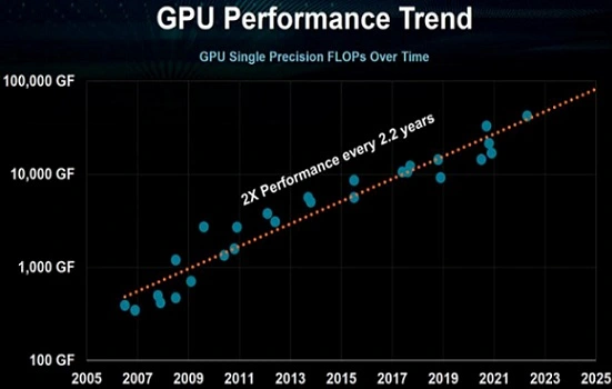
Figure 13: GPU Performance Trend
If you want to get more details, you can check System Architecture | Cloud TPU.

 English










