ASIC (application-specific integrated circuit) is a technology for specialized chip applications. With the development of AI machine learning, edge computing, and autonomous driving, the generation of a large number of data processing tasks has made people put forward high requirements for computing efficiency, computing power, and energy consumption ratio. In order to solve these problems, ASIC chips featuring user participation in design has appeared, which can realize the optimal design of the whole machine system, with superior performance and strong confidentiality. The trend of ASIC chips continues. With ChatGPT exploded, the technology giants such as Google, Intel, and Nvidia successively released ASIC chips such as TPU and DPU. More data shows that the global ASIC chip market is expected to reach US$24.7 bn in 2025, growing at a compound annual growth rate of 8.2% during the forecast period.
ASIC (Application-Specific Integrated Circuit) Basic
ASIC is a chip specially customized for a specific requirement, such as dedicated audio and video processors (get more info from audio devices). At the same time, many dedicated AI chips can be regarded as a type of ASIC.
In semiconductor industry, using CPLD (complex programmable logic device) and FPGA (field programmable logic gate array) to carry out ASIC design is one of the most popular ways. Their commonality is that they all have user field programmable features and support boundary scan technology, but both have their own characteristics in terms of integration, speed and programming methods.
ASIC Features
ASIC is characterized by being oriented to the specific needs of users, with many varieties and small batches, requiring a short design and production cycle. As a product of the close integration of ICs and specific user's complete machine or system technology, it has a larger volume than general-purpose ICs, with advantages of smaller, lighter weight, lower power consumption, improved reliability, sound performance, enhanced confidentiality, low cost and so on.
However, the shortcomings of ASIC chips are also obvious. For example, once the chip is designed, the environment it uses is fixed, it may not be available when requirements change. In addition, because it is a dedicated chip, if the shipment volume is not large, the cost of the chip will be relatively high, due to the larger the shipment volume, the lower the cost.
ASIC Types
According to market demand, ASIC chips can be divided into full-custom, semi-custom and programmable chips.
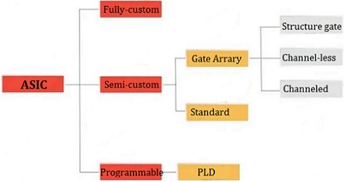
Figure 1: ASIC Types
(1) Full-custom: It is one of the chips with the highest degree of customization. R&D personnel design logic units for functions based on different circuit structures, and build analog circuits, storage units, and mechanical structures on the chip board. With them, full-custom chips are excellent in terms of performance and power consumption. For example, the average computing power output of a fully-custom ASIC chip is about 8 times that of a semi-custom one; and the performance of a fully-custom ASIC chip using 24nm process is better than that of a semi-custom one using 5nm process.
(2) Semi-custom: They can be divided into gate arrays and standard cells. The former include structured gate arrays, channel gate arrays and channelless gate arrays. Most of the logic cells that make up the semi-custom ASIC chip are taken from the standard logic cell library, and some of them are custom designed according to specific needs. In the gate array ASIC chip structure, the positions of predetermined transistors on the wafer cannot be changed, and designers usually adjust the logic unit interconnection structure by changing the metal layer at the bottom of the chip. In addition, designers can arrange standard cells according to algorithm requirements.
(3) Programmable: PLD is also called programmable logic device, which includes basic logic unit matrix, flip-flops, latches, etc. and its interconnection part exists as a single module. And designers program the PLD to meet some custom application requirements.
In terms of hardware, ASIC chips are generally scomposed of silicon materials, gallium phosphide, gallium nitride, etc. In terms of physics, they generally include 32-bit microprocessors, memory and network circuits. To meet the requirements, a chip board can carry one or several ASIC chips with the same or different functions.
ASIC chips can be divided into TPU (tensor processing unit) chips, DPU(data processing unit) chips, and NPU(neural processing unit) chips according to different terminal functions. TPUs are dedicated to machine learning, such as Google's TPU chips. DPUs can provide an engine for computing scenarios such as data centers. NPU is a neural network processor that simulates human neurons and synapses at the circuit level to directly process deep learning instruction sets.
ASIC vs CPU, GPU, FPGA
|
Processor
|
Architecture
|
Features
|
Consumption
|
Flexibility
|
Cost
|
|
CPU
|
Von Neumann architecture
|
Good at logic control and serial operation
|
High
|
Very high
|
High
|
|
GPU
|
Von Neumann architecture
|
Good at parallel computing
|
Very high
|
High
|
High
|
|
FPGA
|
No instructions, no shared memory
|
Have pipelining and parallel processing
|
High
|
High
|
High
|
|
ASIC
|
Customized
|
Low power consumption, well performance
|
Low
|
Low
|
Low
|
Both CPU and GPU are common general-purpose chips that can efficiently complete tasks. However, the difference in design architecture directly leads to the difference in performance of the two chips.
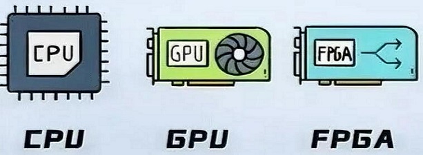
The CPU (central processing unit) is based on a low-latency design and has a strong single-time logical processing capability, but it has limited processing capabilities for large amounts of data with limited power consumption. It requires strong computing power for processing different types of data and logical judgment for branching and jumping, all of which make the internal structure of the CPU extremely complex. In addition, it requires a lot of space for branch prediction and optimization (control), and saves various caches to reduce the delay during task switching. This also makes it more suitable for logic control, serial operations and general type data operations.
GPU (graphics processing unit) is similar to CPU, but it is a kind of microprocessor specialized in image calculation. GPUs are designed to perform the complex mathematical and geometric calculations for graphics rendering. It can provide dozens or even hundreds of times the performance of CPU in some calculations such as floating-point operations and parallel computing. This determines that it is better at handling multiple tasks, especially repetitive tasks without technical content, such as graphics calculations. Since deep learning usually requires a lot of training, the algorithm is not complicated, but the data is very large, and the advantages of multi-core and parallel processing of GPU make it more suitable for deep learning operations than CPU.
It has three limitations: 1) Parallel computing cannot be fully utilized in the application process. 2) The hardware structure is fixed and not programmable. 3) The energy efficiency of running deep learning algorithms is much lower than that of ASIC and FPGA.
FPGA (field programmable gate array) is a semi-custom chip that is always programmable, and users can reprogram it according to their own needs. Compared with GPU and CPU, it has the characteristics of high performance, low energy consumption, and hardware programmable. Even for the logic blocks and connections of the finished FPGA products, users can configure these chips by upgrading the software to realize the required functions without changing the hardware. This also means that the user can quickly program the circuit according to the required logic function. At the same time, it also has its own limitations: 1) The computing power of the basic unit is limited; 2) The speed and power consumption need to be improved; 3) The price of FPGA is relatively expensive.
Different from the flexibility of GPUs and FPGAs, the computing power and efficiency of ASIC chips are directly customized according to the needs of specific algorithms. It has the following advantages:
1) Size: ASIC chips make full use of the unit operation unit function during design to avoid the existence of redundant calculation units, which is conducive to reducing the size of the chip.
2) Energy consumption: The energy consumption per unit computing power of ASIC chips is lower than that of CPU, GPU, and FPGA. For example, GPU consumes about 0.4 watts of power per computing power on average, and ASIC consumes about 0.2 watts at the same time, which can better meet the needs of new smart devices for energy consumption.
3) Integration: Due to the use of customized design, the ASIC chip system, circuit, and process are highly integrated, which helps customers obtain high-performance ICs. For example, TPU v1 is 14-16 times that of traditional GPU, and NPU is 118 times that of GPU. And the Cambrian believes that ASIC will be the core of future AI chips.
ASIC Future
ASIC chips and their supporting products have initially formed an application model in the downstream smart home appliance market, and have a broad market space. By embedding ASIC chips, home appliance manufacturers can obtain higher profits and promote the construction of smart cities.
Google's TPU is between a CPU and a fully-custom ASIC in terms of algorithm architecture, and has the functions of both desktop computing devices and embedded computing devices. The TPU algorithm has higher fault tolerance, and its hardware composition is simpler than that of CPUs. Under the condition of the same number of transistors, the ASIC chip with TPU algorithm architecture can complete a larger amount of calculation. Compared with CPUs and GPUs of the same level, this type of ASIC chip can improve computing performance by 15 to 30 times, and improve energy efficiency by 30 to 80 times. So experts pointed out that the ASIC chip based on the optimized design of the fixed algorithm will become the mainstream core module of the automatic driving computing system.
Because the ASIC algorithm architecture is closer to the underlying algorithm and greatly reduces redundant transistors and connections in the physical structure, ASIC chips outperform conventional chips in terms of computing throughput, delay, power consumption and other parameters. At this stage, the core chip of the autonomous driving system has shifted from GPU to FPGA, and is gradually transitioning to ASIC. Compared with FPGA chips, under the ASIC architecture, the computing efficiency and computing power of the autonomous driving system can be customized. Once it reaches the mass production scale, its average cost will be lower than that of FPGA chips. Under the same process conditions, the calculation speed of ASIC is about 5 times or more than that of FPGA.

 English










