In electronics, there are two main types of video memory, one is GDDR, and the other is HBM (high bandwidth memory). When HBM exists as a GPU memory, it can only be seen on high-end products, because of its high cost. For example, Nvidia's GPUs employed for data centers, and AMD's use of HBM on consumer-grade GPUs is a relatively rare example.
High Bandwidth Memory (HBM)
HBM Basics
Compared with GDDR, HBM is a 3D stacked way that allows vertical layout, so the performance is better in many aspects. First of all, the frequency is low. GDDR6 has already reached the frequency of 20GHz, and the potential for improvement is not great, but HBM only needs 1GHz or even hundreds of MHz to have stronger performance, because the memory width of HBM is relatively large. For example, the current RTX3090 is 384-bit, which is already a ceiling, but HBM can achieve a bit width of 4096bit. Of course, this means that HBM can easily bring super large bandwidth, and with the advancement of technology, the frequency of HBM2 can reach 2GHz, and HBM3 will be reach 4GHz, so this means that HBM memory can easily achieve a bandwidth rate of 1TB/S.
Except that, the HBM is smaller in size and lower in power consumption. Low power consumption can save more power. This has little impact on high-power electrical appliances such as graphics cards, but the small size is very helpful. This allows HBM does not need to occupy the space of the PCB board, because the HBM and the graphics card core are directly packaged together, which can save a lot of space.
Back then, AMD’s Fury X used such a thin body to achieve a more powerful output. It can be seen that the advantages of HBM memory, and the subsequent HBM3 indicators are doubled compared to HBM2, although GDDR is also being upgraded, but the potential is getting smaller and smaller. GDDR6 can theoretically achieve a memory frequency of 20GHz, and is already difficult to continue to improve, but HBM is much easier. Where the development direction of HBM is similar to 3D NAND.
HBM Matches with CPU?
Some gamers should know that HBM is a high-speed memory with a bandwidth far exceeding DDR/GDDR, and the internal structure also uses 3D stacked SRAM. So some people have thought that if HBM can be used in personal computers and notebook products, and matched with general CPUs, their performance can be greatly enhanced. But in reality, the cost is high, and the GPU is already using HBM.
In fact, the CPU that matches with HBM exists. For example, the chip A64FX used in Fujitsu's supercomputer Fugaku is equipped with HBM2; Intel's Sapphire Rapids Xeon processors have an HBM memory version; and NEC SX-Aurora TSUBASA is also the same, etc.
Therefore, it is feasible for the CPU to be used with HBM (although in a strict sense, chips such as A64FX have surpassed the scope of the CPU), but these products are still oriented to data centers or HPC applications. Is it because of the high price that HBM has not been distributed to the consumer market? This may be an important or relatively close to the truth. In this article, we will talk about the characteristics and usage scenarios of HBM, and whether it will replace the common DDR memory in the future.
As far as the common form of HBM is concerned, it usually exists in the form of several dies on the surface, next to the main chip (such as CPU, GPU). For example, in the picture below, the four packages around the A64FX are all HBM memory. Such an existence form is quite different from ordinary DDR memory.
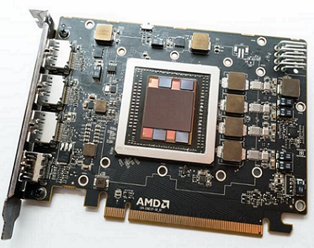
Figure 1: AMD Radeon R9 Nano
One of the characteristics of HBM is to achieve higher transmission bandwidth with smaller size and higher efficiency (partial) than DDR/GDDR. And in fact, each HBM package has many layers of DRAM die stacked inside, so it is also a 3D structure. The DRAM dies are connected by TSV (through-silicon vias) and microbumps, in addition to the stacked ones, there will be an HBM controller logic die on the lower layer. Then the lowest layer is interconnected with CPU/GPU through base die (for example, silicon interposer).
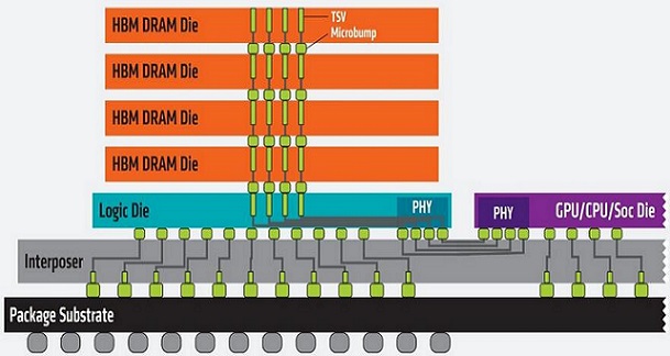
Figure 2: HBM Memory Structure (side view) (Source: AMD)
From this structure, it is not difficult to find that the interconnection width is much larger than that of DDR/GDDR, and the number of contacts interconnected below can be far more than the number of lines connecting DDR memory to CPU. The scale of the PHY interface of HBM2 is not at the same level as the DDR interface, and the connection density of HBM2 is much higher. From the perspective of transmission bit width, each layer of DRAM die has two 128-bit channels, and the HBM memory with 4 layers of DRAM die height has a total bit width of 1024-bit. Many GPUs and CPUs have four such HBM memories around them, and the total bit width is 4096-bit.
As a comparison, the bit width of each channel of GDDR5 memory is 32-bit, the total bit width of 16 channels is 512-bit, and the total bit width of DDR4 is common. In fact, the current mainstream second-generation HBM2 can stack up to 8 layers of DRAM die per stack, which improves the capacity and speed more. Each stack of HBM2 supports up to 1024 data pins, and the transmission rate of each pin can reach 2000Mbit/s, so the total bandwidth is 256Gbyte/s. Under the transmission rate of 2400Mbit/s for each pin, the bandwidth encapsulated by an HBM2 stack is 307Gbyte/s.
The figure below is a comparison of DDR, LPDDR, GDDR and HBM given by Synopsys. You can look at the Max I/F BW column. They are not in the same order of magnitude as HBM2. With such a high bandwidth, it must be very good to run on applications such as highly parallel computing, computer vision, and AI. And from an intuitive point of view, HBM and the main chip are so close, theoretically, higher transmission efficiency can be obtained (from the perspective of energy consumed per bit of data transmission, HMB2 does have a great advantage).
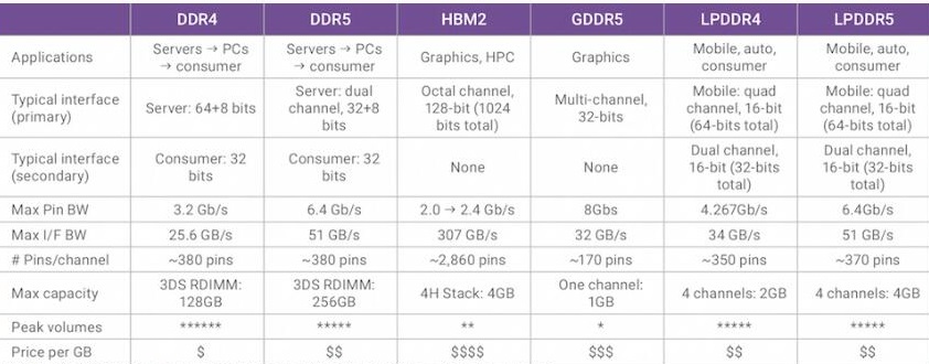
Figure 3: HBM vs DDR, LPDDR, GDDR
It can be seen that the disadvantage of HBM lies in the cost and the total memory capacity. If it is really used as memory in a personal computer, is it perfect? But why AMD give up? In fact, it is because of the cost. Although graphics cards are very expensive, for manufacturers, the cost must be saved as much as possible. In addition, a graphics card worth 1,000 U.S dollars is already very high-end for ordinary users, but in the field of professional computing, it's not enough.
In fact, this is quite reasonable, the parameters of HBM are very good, but the actual experience does not bring much perception. In those days, AMD used HBM lost to Nvidia’s GDDR5, so it doesn’t matter whether it is used or not. Even if HBM is used, the graphics card’s game performance has not much improvement. In addition, Nvidia products themselves are very cost-effective, so AMD uses HBM memory is in bad situation.
However, HBM is still used a lot in the field of professional high-performance computing. For ordinary game cards, the biggest advantage may be that it can save some space on the PCB board and reduce the length of the graphics card. Not to mention GDDR6, for many people, GDDR5 and even GDDR3 are still be used properly. After all, for graphics cards, the architecture and process of them are more important. As for the impact of video memory on performance, it is the same as the impact of memory on CPU, but not as important as people imagined.
However, with the development of technology, HBM must gradually replace GDDR. After all, it has great potential, as long as the cost can be reduced.
HBM Disadvantages
The real problem is that HBM also has many shortcomings:
1) Poor Flexibility
HBM was first initiated by AMD in 2008, and its original purpose is to make changes in power consumption and size of computer memory. In the following years, AMD has been trying to solve the technical problems of die stacking, and later found partners with storage media stacking experience in the industry, including SK Hynix, and some manufacturers in the field of interposer and packaging.
Then in 2013, it was first produced by SK Hynix. And this year, HBM was adopted by the JESD235 standard of JEDEC memory standards. The first GPU to apply HBM storage was AMD Fiji (Radeon R9 Fury X) in 2015, and Samsung began mass production of HBM2 in the following year - Nvidia Tesla P100 was the first GPU to adopt HBM2 storage.
From the form of HBM, it is not difficult to find its first shortcoming: the lack of flexibility in system collocation. For PCs in the early years, the expansion of memory capacity was a relatively routine. However, HBM is packaged with the main chip, and there is no possibility of capacity expansion, and the specifications have been fixed before leaving the factory. Moreover, it is not the same as the DDR memory soldered on the motherboard on the current notebook equipment. HBM is integrated on the chip by the chip manufacturer-its flexibility will be weaker, especially for OEM manufacturers. (Although some high-end systems now may have HBM+DDR solutions, the two types of memory are allocated as different levels of storage systems).
For the vast majority of chip manufacturers, it is unlikely to launch chip SKU models with various memory capacities based on various considerations including cost to promote processors for the mass market. The processors promoted by these manufacturers have various configuration models (for example, Intel Core processors have various models)-if you consider the difference in subdivided memory capacity, the manufacturing cost may be difficult to support.
However, in the consumer market, users who pay more attention to portability may not care much about the scalability of memory. For example, the Apple M1 is a typical representative, and the 8GB/16GB memory is on the side of the M1 chip. Among consumer products, one of the few products that will package memory on the chip is Intel LakeField. Both chips do sacrifice memory scalability. But even luxury products such as Apple M1 and Intel Lakefield do not actually use HBM memory (of course, the packaging method of both is not a 2.5D package like silicon poser).
2) Small Capacity
The second problem with HBM is that memory capacity is more limited than DDR. Although one HBM package can stack 8 layers of DRAM die, in fact, each layer is only 8Gbit, so 8 layers is 8GByte. A supercomputing chip like A64FX has 4 HBM interfaces, and it has a total capacity of 32GByte.
Such a capacity is still too small compared with DDR. It is really common for ordinary PCs in the consumer market to heap more than 32GByte of memory. Not only are there a large number of expandable memory slots on PC and server motherboards, but some DDR4/5 DIMMs memory particles are also stacking DRAM die. Using a relatively high-end DRAM die stack, 2-rank RDIMMs (registered) can achieve a capacity of 128GByte—considering 96 DIMM slots in a high-end server, that is a capacity of up to 12TByte.
Of course, as mentioned earlier, HBM and DDR can be mixed and used together. For example, HBM2 is responsible for high bandwidth but small capacity, and DDR4 is responsible for slightly lower bandwidth but large capacity. From the perspective of system design, the HBM2 memory is more like a L4 cache in the processor.
3) High Latency
For PCs, an important reason why HBM has not been applied to CPU main memory is its high latency. Although many popular science articles will say that its delay is not a big problem. For example, Xilinx describes its delay as similar to DDR for FPGAs equipped with HBM, but the "delay" mentioned in many articles may not be the same.
Common DDR memory is generally marked with CL (column address strobe CAS delay, the clock cycle required for column addressing, to indicate the length of read delay) in the specifications. Where the CAS delay refers to the waiting time from the time when the read command is issued to the time when the data is ready.
After the memory controller tells the memory that data at a specific location needs to be accessed, which will take several cycles to arrive at the location and execute the instructions issued by the controller. CL is the most important parameter in memory latency. In terms of delay length, the "cycle" here actually needs to be multiplied by the time per cycle (the higher the overall operating frequency, the shorter the time per cycle).
For HBM, as mentioned earlier, one of its characteristics is ultra-wide interconnection width (or too many parallel transmission lines), which determines that the transmission frequency of HBM should not be too high, otherwise the total power consumption and heat generation will be high.
The frequency of HBM is indeed much lower than that of DDR/GDDR. For example, the transmission bandwidth of each pin of Samsung’s previous Flarebolt HBM2 memory is 2Gbit/s, and the frequency is almost 1GHz. Later, there are products that boost the frequency to 1.2GHz. Samsung mentioned at the time that this process also needs to consider reducing the parallel clock interference between more than 5,000 TSVs; and it needs to increase the heat dissipation bumps between DRAM dies to alleviate the heating problem.
Previously, Zhejiang University and ETH Zurich published a paper entitled Benchmarking High Bandwidth Memory on FPGA. This paper mainly studies the detailed characteristics of HBM on FPGA and how to improve the efficiency of FPGA based on these characteristics. This study was based on Xilinx's Alveo U280 - an FPGA with two stacked HBM subsystems on top.
|
Idle Latency
|
HBM
|
DDR4
|
|
Cycles
|
Time
|
Cycles
|
Time
|
|
Page hit
|
48
|
103.7 ns
|
22
|
73.3 ns
|
|
Page closed
|
55
|
122.2 ns
|
27
|
89.9 ns
|
|
Page miss
|
62
|
137.8 ns
|
32
|
106.6 ns
|
Source: Benchmarking High Bandwidth Memory on FPGA
This paper specifically mentioned: "The delay of HBM is much higher than that of DDR4. The connection between the HBM chip and the corresponding FPGA is made through a serial I/O connection, which requires parallel-serial-parallel conversion processing." The above table is the memory access delay between HBM and DDR4 presented in this study. The page hit here means that there is no need for Precharge and Activate instructions before the memory column access (the bank is in the open state when the row is accessed), and the minimum delay can be achieved. For details such as page closed/miss, please refer to the original text.
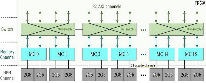
Figure 4: Architecture of Xilinx HBM Subsystem (source: Benchmarking High Bandwidth Memory on FPGA)
Perhaps from a system point of view, Alveo U280 has certain particularities, but it should still be able to expose the problem. Each HBM stack inside is divided into 8 independent memory channels (the aforementioned 4-layer DRAM die), and each memory channel is further divided into two 64bit pseudo channels. In addition, other systems that include HBM are also structured in a similar way.
On top of a total of 16 memory channels, 32 AXI channels interact with user logic: each AXI channel provides a standard interface for FPGA programming, and only allows access to its own memory region. In order to allow each AXI channel to access the complete HBM space, Xilinx introduced a switch between channels. In short, wider bit widths and more complex systems are always important factors that cause HBM access delay.
Is HBM Suitable for PCs?
The characteristics of high bandwidth and high latency determine that HBM is very suitable for GPU, because games and graphics processing are highly predictable and concurrent tasks. The characteristic of this type of load is that it requires high bandwidth and is not so sensitive to latency. So HBM will appear on high-end GPU products. According to it, HBM is actually very suitable for HPC high-performance computing and AI computing. Therefore, although A64FX and the next-generation Xeon processor are CPUs, they will also choose to consider using HBM as memory.
But for PCs, the tasks to be processed by the CPU are extremely unpredictable, requiring various random storage accesses, and are inherently more sensitive to delays; and the requirements for low latency are often over than those for high bandwidth. All in all, it is difficult for HBM to replace DDR on PCs in the short term. It seems that this question is also similar to whether GDDR can be applied to PC memory.
But in the long run, no one can predict the situation. As mentioned above, a mixed solution can be considered, and the storage resources of different levels are undergoing significant changes. For example, AMD has piled up the L3 cache on the processor to 192MB. For the cache in the die, which is a component that hides the delay of external storage, it may be that as the cache on the processor chip becomes larger, the delay requirements for system memory are not so high.

 English










