Nvidia has developed a series of graphics processing unit (GPU) microarchitectures to improve computing performance. A GPU consists of hundreds of smaller cores, they operate to crunch through the data in the application.Here you may have a question, which architecture is a GPU using? how does it look like?
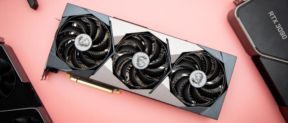
Terminology
GPU (graphics processing unit) is a general-purpose graphics processor. Due to the use of multi-core parallel computing infrastructure and a large number of cores, it can support parallel computing of a large amount. What’s more, because of high data bandwidth, high-speed memory access, and high floating-point computing capabilities, it is widely used in the training and inference of deep learning AI models, especially in the field of training, where Nvidia's GPU solution currently takes the first place. Every 2 to 3 years, Nvidia will launch a new generation of GPU architecture, from Tesla in 2008 to Volta in 2018 to the latest Ampere. Through the evolution of the architecture, the computing power of each generation of GPU will be greatly improved. The following will sort out the development of Nvidia's GPU architectures.
As of 2021, the 8 NVIDIA GPU architectures are as following:
• Tesla
• Fermi
• Kepler
• Maxwell
• Pascal
• Volta
• Turing
• Ampere
• Hopper
NVIDIA generally names its GPU architecture after some famous scientists in history.
GPU Architecture Details
The Tesla Architecture
There is not much info about the Tesla architecture on the official website, and it is NVIDIA's first architecture to implement a unified shader model, while the classic model is the G80. If you want to check, there is a brief introduction to the G80 in the opening part of the Fermi architecture white paper.
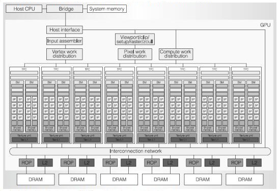
Figure 1: Tesla Architecture, Chip G80 Reference
1) G80 is the first GPU that supports C language, allowing programmers to use the powerful functions of the GPU without learning a new programming language.
2) The G80 is the first GPU to replace separate vertex and pixel pipelines with a single, unified processor that can execute vertex, geometry, pixel, and compute programs.
3) The G80 is the first GPU to use a scalar thread processor, eliminating the need for programmers to manually manage vector registers.
4) G80 introduces a single instruction multiple thread (SIMT) execution model, that is, multiple independent threads execute concurrently using one instruction.
5) G80 introduces shared memory and barrier synchronization for inter-thread communication.
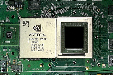
Figure 2: G80 GPU Chip
The Fermi Architecture
The Fermi architecture is the most significant leap since the original G80. NVIDIA's GPU R&D team took lessons learned from the G80 and GT200 models and found a new design approach to create the world's first computing GPU, improving the following key areas:
1) Increased double-precision- While single-precision floating-point performance is roughly ten times that of a desktop CPU, but some computing applications also have requirement.
2) ECC support - It allows GPU computing users to safely deploy large numbers of GPUs in data center installations and ensure data-sensitive applications such as medical imaging and financial options pricing are immune to memory errors.
3) True Cache Hierarchy - Some parallel algorithms cannot use the shared memory of the GPU, and users need a real cache architecture to help them.
4) More shared memory - Many CUDA programmers require more than 16KB of SM shared memory to speed up their applications.
5) Faster context switching - Users are demanding faster context switching between applications and faster graphics and compute interoperability.
6) Faster Atomic Operations - Users requested faster read-modify-write atomic operations for their parallel algorithms.
Based on the above points, the Fermi architecture has the following four highlights:
1) Third-gen streaming multiprocessor (SM)
a. Each SM has 32 CUDA cores, 4 times that of GT200
b. 8 times the peak double-precision floating-point performance of GT200
c. Dual warp scheduler simultaneously schedules and dispatches instructions from two independent warps
d. 64Kb RAM, configurable shared memory and L1 cache
2) The second-gen of parallel thread execution ISA
a. Unified address space with full C++ support
b. Optimized for OpenCL and DirectCompute
c. Full IEEE 754-2008 32-bit and 64-bit precision
d. Full 32-bit integer path with 64-bit extensions
e. Memory access instructions that support the transition to 64-bit addressing
f. Improving performance through prediction
3) Improved memory subsystem
a. NVIDIA Parallel DataCache TM hierarchy with configurable L1 and Unified L2 Caches
b. The first GPU to support ECC memory
c. Significantly improve the performance of atomic memory operations
4) NVIDIA GigaThread engine
a. Application context switching speed increased by 10 times
b. Concurrent Kernel Execution
c. Out-of-order thread block execution
d. Dual overlapping memory transfer engine
The above are the improvements of the Fermi architecture compared to the original architecture. Let's take a look at the configuration of the Fermi in detail:
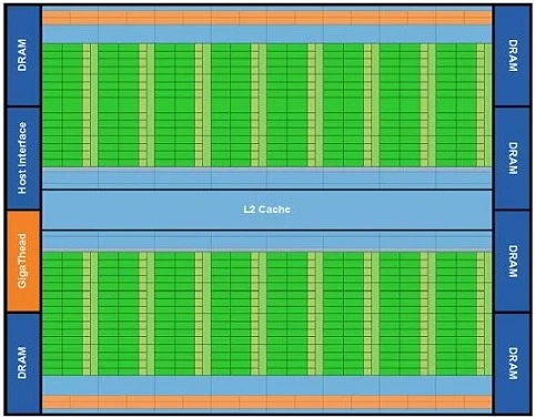
Figure 3: NVIDIA Fermi GPU Architecture
The first GPU based on the Fermi architecture, had 3 billion transistors and a total of 512 CUDA cores. They are organized into 16 SMs, and each one is a vertical rectangular strip (content in the red box) with 32 CUDA cores, located around a common L2 cache. In addition, a CUDA core executes one floating-point or integer instruction per clock cycle for a thread.
Six 64-bit video memory partitions form a 384-bit video memory interface, supporting a total of up to 6GB of GDDR5 DRAM video memory. The host interface connects the GPU to the CPU via PCI-Express. And the Giga Thread global scheduler distributes thread blocks to the SM thread scheduler.
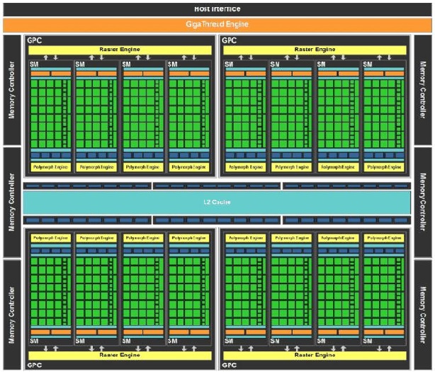
Figure 4: Fermi Graphics Rendering Architecture
The entire GPU has multiple GPCs (graphics processing clusters), and each one contains a raster engine, four SMs, and the GPC can be considered as an independent GPU. All NVIDIA GPUs, starting with Fermi, have GPC.
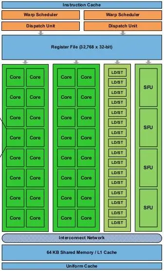
Figure 5: Fermi Streaming Multiprocessor (SM)
The picture above is a detailed structural diagram of one of the 16 SMs taken out and enlarged, including:
a. Orange : 2 Warp scheduler/Dispatch units
b. Green: 32 CUDA cores, divided into two lanes, each with 16
c. Light blue part: register file and L1 cache
d. 16 Load/Store units (LD/ST Unit)
e. 4 special function units (SFU)
f. Each SM has 32 CUDA cores, which is green in the picture, and each has a fully pipelined integer arithmetic logic unit (ALU) and floating point unit (FPU):
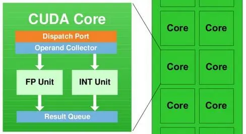
Figure 6: CUDA Core
Streaming Multiprocessor is a very important part of the GPU architecture, and the parallelism of the GPU hardware is determined by the SM.
The Kepler Architecture
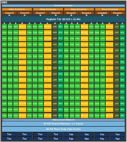
Figure 7: NVIDIA Kepler Architecture
The idea of the Kepler architecture is to reduce the number of SM units (called SMX units in this gen) and increase the number of CUDA cores in each group of SM units. In addition, the number of CUDA cores per SM unit has increased from 32 to 192.
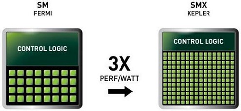
Figure 8: NVIDIA Kepler Architecture with 192 Cores
a. In each SMX:
b. 4 warp schedulers, 8 dispatch units
c. 32 SFUs
d. Green: 192 CUDA cores, divided into 12 lanes, each with 16 lanes
e. Yellow: 64 DP double-precision arithmetic units, divided into 4 lanes, and 32 LD/ST Units
The Maxwell Architecture
Compared with the Kepler architecture, the SM unit of the Maxwell architecture has changed a lot. The SM unit of it is more like four SM units of the Fermi architecture arranged together in a 2x2 manner. This generation is called the SMM unit:
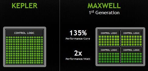
Figure 9: Maxwell Streaming Multiprocessors Compared with Kepler
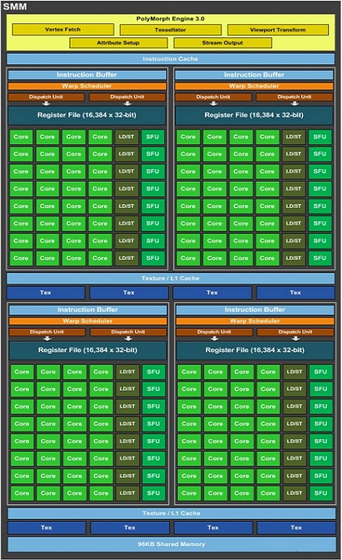
Figure 10: NVidia Maxwell Architecture
The SMM uses a quadrant-based design with four 32-core processing blocks, each with a dedicated warp scheduler capable of dispatching two instructions per clock.
Each SMM unit provides
a. 8 texture units
b. A polymorph engine (graphic geometry processing)
c. Special register files and shared memory
In each processing block:
a. 1 warp scheduler, 2 dispatch units
b. Green: 32 CUDA cores
c. 8 LD/ST units
d. 8 SFUs
The total number of CUDA cores has been reduced from 192 per group of SM units in the Kpler era to 128, but each SMM unit will have more logic control circuits for precise control.
The Pascal Architecture
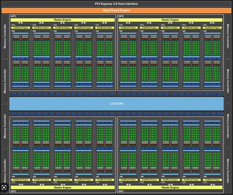
Figure 11: NVIDIA Pascal Architecture Diagram
Different NVIDIA architectures have several different cores. The Pascal architecture has two major cores: GP100 and GP102:
* GP100: 3840 CUDA cores, 60 sets of SM units
* GP102: 3584 CUDA cores, 28 sets of SM units
The core is a complete GPU module, the figure above shows the GP100 core with 60 SM units. Different graphics card products can use different GP100 configurations, which are usually full or reduced. For example, Tesla P100 uses 56 SM units.
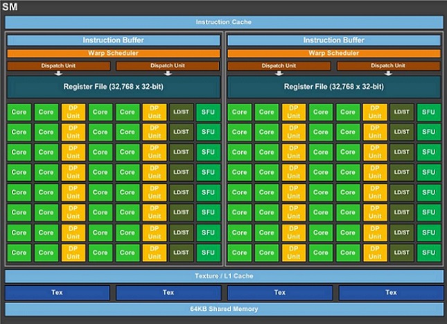
Figure 12: SM Unit at the Core of GP100
Each SM unit is divided into 2 Process Blocks, and in each one:
a. 1 warp scheduler, 2 dispatch units
b. Green: 32 CUDA cores
c. Yellow: 16 DP double-precision arithmetic units on 2 lanes, and each lane has 8 units
d. 8 LD/ST units
e. 8 SFUs
The total number of Maxwell CUDA cores has been reduced from 128 per group of SM units to 64 per group. The biggest feature of it is the comeback of DP double-precision arithmetic units. The process technology has been upgraded to 16nm, and the performance has been greatly improved, but the power consumption has not increased.
The Volta Architecture
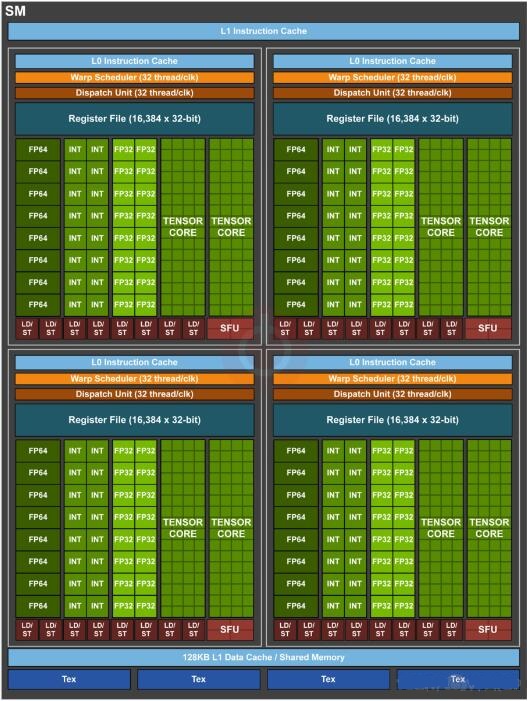
Figure 13: Nvidia GV100 SM Units
Each SM unit is divided into 4 Process Blocks, and in each one:
a. 1 warp scheduler, 1 dispatch unit
b. 8 FP64 cores
c. 16 INT32 cores
d. 16 FP32 cores
e. 2 tensor cores
f. 8 LD/ST units
g. 4 SFUs
In previous architectures, a CUDA core could only execute one floating-point or integer instruction per clock cycle for a thread. But starting from the Volta architecture, a CUDA core is split into two parts: FP32 and INT32. The advantage is that in the same clock cycle, floating-point and integer instructions can be executed at the same time to improve the calculation speed. In addition to the traditional single and double precision calculations, the Volta also adds a dedicated tensor core tensor unit for deep learning and AI operations.
The Turing Architecture
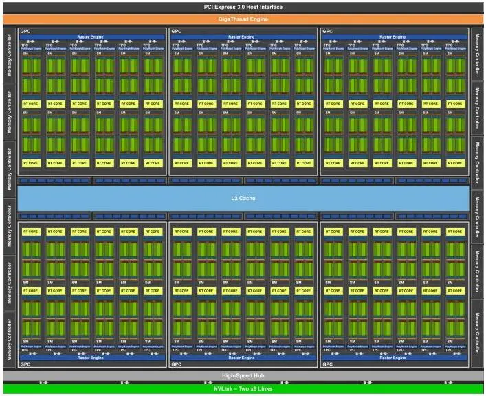
Figure 14: Nvidia Turing Architecture (TU102 Core)
The Turing architecture currently has three cores:
* TU102 core * TU104 core * TU106 core
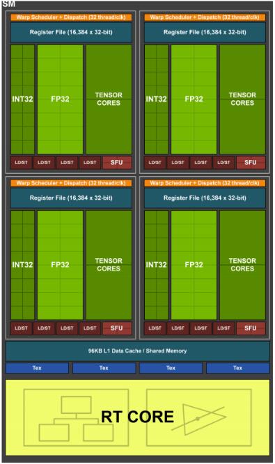
Figure 15: Nvidia TU102 SM Units
Each SM unit has 4 processing blocks, and in each one:
a. 1 warp scheduler, 1 dispath unit
b. 16 INT32 cores
c. 16 FP32 cores
d. 2 Tensor cores
e. 4 LD/ST units
f. 4 SFUs
The Turing architecture doesn’t support FP64.
The Ampere Architecture
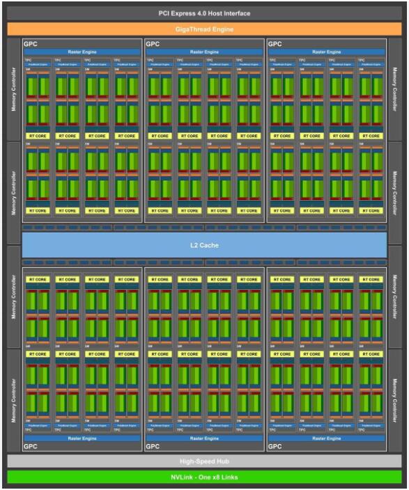
Figure 16: Nvidia Ampere Architecture (GA102 Core)
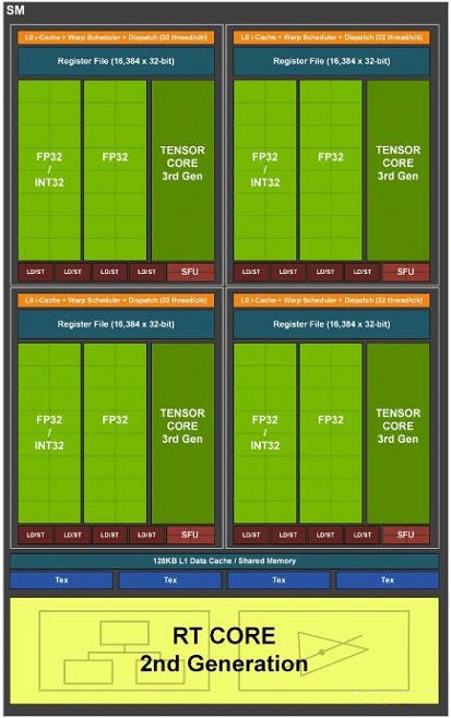
Figure 17: Nvidia GA102 SM Units
Each SM unit is divided into 4 processing blocks, and in each one:
a. 1 warp scheduler, 1 dispatch unit
b. 8 FP64 cores
c. 16 FP32 cores
d. 16 INT32 cores
e. 1 tensor core
f. 8 LD/ST units
g. 4 SFUs
The Ampere has added FP64 core back. At the same time, since the Volta architecture, it is the third-generation Tensor technology, so Nvidia maintains an Tensor update in every generation.
The Hopper Architecture
The NVIDIA H100 chip adopts TSMC's 4-nm process (an optimized version of N5 process), with a core area of 814 square millimeters, which is 14 square millimeters smaller than the A100. Although the core area is smaller, the number of transistors has increased from 54.2 billion to 80 billion due to to the 4nm process.
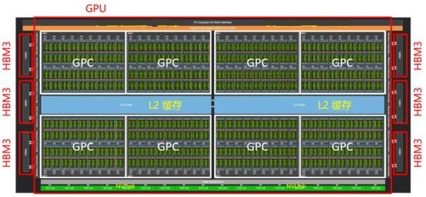
Figure 18: NVIDIA Hopper H100
Judging from the core design diagram, the Hopper architecture is similar to Apple UltraFusion, but it is essentially a single chip, rather than the Apple M1 Ultra that bridges two chips. The top-level topology is not much different from the Ampere architecture. The Hopper GPU is composed of 8 graphics processing clusters (GPCs), and each of the 4 GPCs shares a 25MB L2 cache. On both sides of the core is HBM3 memory, which has a bit width of 5120 bits and a maximum capacity of 80Gb.
Each GPC on the chip is composed of 9 texture processor clusters (TPC), and the computing tasks entered by PCIe5 or interface are distributed to each GPC. GPC shares intermediate data through L2 cache, and the intermediate data calculated by GPC communicates with other GPUs through NVLink. Each TPC consists of 2 SM units.
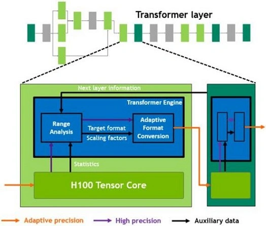
Figure 19: NVIDIA H100 Transfer Layer
The performance improvement and major changes of the Hopper are reflected in the new thread block cluster and a new SM unit. Because of a new thread block cluster mechanism, which enables collaborative computing across units. At the same time, the thread block cluster in H100 can run a large number of concurrent operations in the same GPC, and has better acceleration ability for larger models.
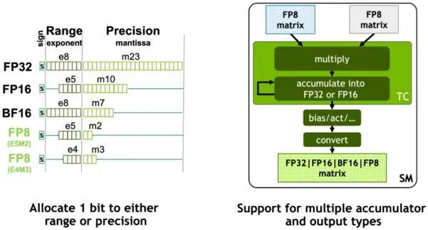
Figure 20: Two FP8 Formats Available by Hopper Architecture
Each includes 128 FP32 CUDA cores, 4 4th-gen Tensor cores. The instructions of each unit are first stored in the L1 instruction cache, and then distributed to the L0 instruction cache. The thread warp scheduler and the dispatch unit that are matched with the L0 cache, which allocates computing tasks for the CUDA core and the tensor core. By using 4 special function (SFU) units, perform transcendental function and interpolation function calculations.
NVIDIA introduced a new generation of streaming multiprocessor FP8 tensor core in the Hopper architecture to accelerate AI training and inference. And FP8 tensor core support FP32 and FP16 accumulators and two FP8 input types (E4M3 and E5M2). Compared to FP16 or BF16, FP8 halves data storage requirements and doubles throughput. In the analysis of the Transformer engine, it will also be seen that the use of FP8 can adaptively increase the calculation speed.
In the GPU, the key module of tensor core AI acceleration is also different from Ampere and later GPU architectures and early GPUs. Tensor Cores are dedicated high-performance computing cores for Matrix Multiply-Accumulate (MMA) math operations, delivering breakthrough performance acceleration for AI and HPC applications.
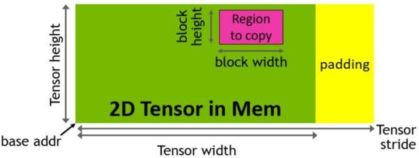
Figure 21: Matrix Multiply-Accumulate MMA
Hopper's tensor cores support FP8, FP16, BF16, TF32, FP64, and INT8 MMA data types. The key point of this generation of tensor cores is the introduction of the Transformer engine. The Transformer operator is the basis of mainstream NLP models such as BERT to GPT-3, and is increasingly used in different fields such as computer vision and protein structure prediction.
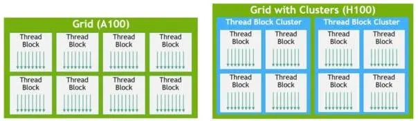
Figure 22: Grid (A100) vs Grid with Clusters (H100)
Compared with the previous A100, the new Transformer engine combined with the Hopper FP8 tensor core provides up to 9 times faster AI training and 30 times faster AI inference on large NLP models. In order to improve the calculation efficiency of Transformer, use mixed precision to intelligently manage the calculation precision during the calculation process. In each layer of Transformer calculation, according to the next layer of neural network layer and the required precision, the FP8 and other floating perform dynamic format conversion in the dot format, making full use of the computing power of the tensor core.
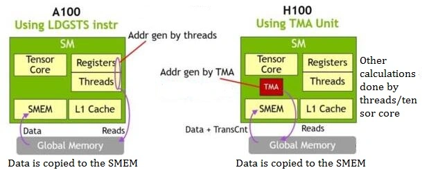
Figure 23: A100 Using LDGSTS Instr vs H100 Using TMA Unit
A new tensor memory accelerator (TMA) has been added to the Hopper architecture to improve the data exchange efficiency between tensor cores, global storage and shared storage. The new TMA uses tensor dimensions and block coordinates to specify data transfers, rather than simple addressing according to data address. What’s more, it significantly reduces addressing overhead and improves efficiency by supporting different tensor layouts, different memory access patterns.
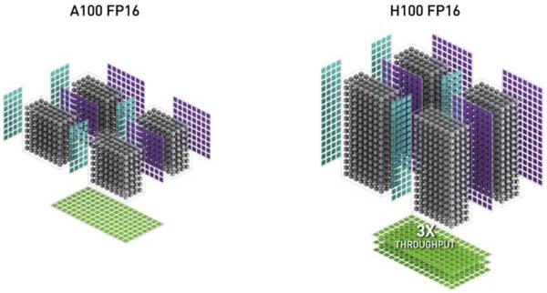
Figure 24: A100 FP16 vs H100 FP16
The TMA operation is asynchronous, multiple threads can share the data channel, and data transmission can be done by sorting. The key advantage of TMA is that it can release the computing power of threads to perform other tasks. For example, in terms of A100, the thread itself is responsible for generating all addresses and doing all data copy operations; but TMA in Hopper is responsible for generating address sequences (this idea is similar to DMA controller), taking over the task of data copying, and letting threads do other things.
Compared with the A100, the computing performance of the H100 is about 6 times higher. The core reason for the substantial performance improvement is that the FP8 tensor core and the Transformer engine for NLP tasks, to reduce the useless work of the unit during data replication.

 English










