In computer architecture, a bus is a set of common information transfer lines that can be time-shared by multiple components. Time sharing and sharing are two characteristics of the bus. Because there are so many components that need to be connected to each other in a modern computer, it is too difficult and costly to connect each component separately, so it is necessary to introduce a common path to realize the connection function of each component.
Bus Basics
Bus Architecture
The characteristics of the multi-bus architecture:
1) It is connected to each other through the bridge, CPU bus, system bus and high-speed bus.
2) The information transmission of the major components is not only through the system bus.
3) It reflects that high-speed, medium-speed and low-speed devices are connected to different buses at the same time to improve the efficiency and throughput of the bus.
4) The change of the processor structure does not affect the high-speed bus.
5) The speed of the bus near the CPU is faster, and the speed of the bus near the I/O interface is slower.
Bus Types
1) On-chip Bus
It is the bus inside the chip, which is the common connection between registers and registers inside the CPU chip, and between registers and ALU.
2) System Bus
It is the bus that connects the various functional components in the computer (such as CPU, main memory and IO devices). It is classified as follows:
Data bus: It is used to transmit data information between functional components. It is a two-way transmission bus. The number of bits is related to the machine word length and storage word length.
Address bus: It is used to transmit the address of data in the main memory unit or I/O port. It is a one-way transmission bus. The number of bits of the address bus is related to the size of the main memory address space.
Control bus: It is used to transmit control information, including control commands sent by the CPU and feedback signals returned by the main memory (or peripherals).
3) I/O Bus
It is mainly used to connect low-speed I/O devices, and is connected to the system bus through the I/O interface. The purpose is to separate low-speed devices from the high-speed bus to improve the system performance of the bus.
4) Communication Bus
It is a bus that transmits information between computer systems or between a computer system and other systems. The communication bus is also called an external bus.
Other categories: synchronous bus, asynchronous bus, parallel bus, serial bus.
Comparison between serial bus and parallel bus: The serial bus can only transmit one bit of data at a time, while the parallel bus can transmit multiple bits of data at a time. However, it does not mean that the transmission speed of the parallel bus must be higher than that of the serial's. The reasons are as follows:
When the actual clock frequency is low, the parallel bus is indeed faster than the serial bus because it can transmit several bits at the same time, but as the clock frequency increases, when transmitting at a high clock frequency, the interference between the parallel buses will be serious, and even the transmitted data be damaged. Parallel bus lines are many and complex, serial bus lines are less, so interference is easy to control.
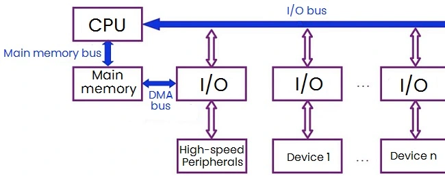
Figure 1: Computer System Bus
Bus Information Transmission Method
Bus transaction
The process of a transfer on the bus is divided into five parts: transfer request, bus arbitration, component/device addressing, data transfer and bus release.
1) Request: the master device issues a bus transmission request and obtains bus control.
2) Arbitrate: the bus authority decides to grant the bus usage right for the next transmission cycle to an applicant.
3) Address: the master device gives the address and related commands of the slave device to be accessed through the bus, and starts the slave module.
4) Transmit: the master module and the slave module exchange data, and data transmission can be performed in one direction or in two directions.
5) Release: the relevant information on the main module is withdrawn from the system bus, giving up the bus usage right.
Bus Data Transmission Mode
1) Parallel transmission mode: Each bit of data is transmitted simultaneously using multiple data lines, with the features of high transmission rate, high cost, and limited transmission distance.
2) Serial transmission mode: Each data is transmitted by one data line, with the characteristics of low transmission rate, long transmission distance, few data lines, and low cost.
3) Time-sharing transmission mode: It refers to using the same signal line on the bus to transmit different information at different time periods, also known as time-division multiplexing.
4) Message transmission mode: Message transmission transmits data packets in bursts. The burst mode is a means of continuously transmitting data using one address segment and multiple data segments in the same bus cycle, and can continuously transmit data. Messaging enables more and faster information delivery in one pass. And PCI, USB use message passing.
Bus Communication Method
1) Synchronous communication
The sending and receiving parties share the same clock, and transmit according to the common clock frequency. And use a fixed transport protocol, which is used for communication associated with the clock.
Disadvantages
a. Every device on the bus must use the same clock frequency, which is determined by the slowest device.
b. Due to the clock skew problem, the length of the high-speed synchronous communication bus cannot be too long.
2) Asynchronous communication
It is not suitable for common clock timing, and there is no clock line in the bus, which overcomes the two shortcomings of the synchronous communication bus. A handshake protocol is used to coordinate the transfer of data between the sending device and the receiving device. Typical handshake signals are:
Data ready (DATA RDY)/request (REQ) and response (ACK), there are three different protocols for the two handshake signals: non-interlocked, semi-interlocked, and fully interlocked.
Development of On-Chip Buses
Introduction
Why does the CPU need an on-chip bus? Because the bus connects the various modules inside the die, it is a necessary way for information exchange between them. Whether its design is efficient or not will greatly affect the performance of the CPU. If we regard each module as a node, then the interconnection relationship between them can generally have the following types:
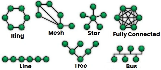
Figure 2: Interconnect Architectures Diagrams
And the CPU on-chip bus connection has gone through the process from star connection --> ring bus --> mesh network.
Star Connection
The number of internal modules of the early CPU was small, and the structure was single. Star connection is a simple and efficient method.
The core of the computer is undoubtedly placed at the center, and all modules are connected to it, but do not directly interact with each other, and must be relayed by the core. This design is simple and efficient and has been used for quite a long time.
The problem increases with the emergence of multiple cores, that is, where should the extra cores be placed? A variant of the star connection is used. It is similar to a binary star structure, the middle node seems to be split, divided into two, each in charge of its own sphere of influence. At the same time, for the sake of efficiency, each core extends some tentacles to connect with other cores. Then this problem is temporarily solved, and this confusing relationship is fixed until the number of cores increases further.
Intel’s Ring Bus to Mesh Interconnect
Ring Bus
Intel's servers were the first to suffer from such a chaotic arrangement. For example, the Xeon processors can have more CPUs, but the inefficient variant star connection limits the increase in the number of cores. Coupled with the increasing demand for communication between modules, a new bus was born.
In the epoch-making product of Nehalem EP/EX, many new technologies have been introduced, and Ring Bus is one of the important ones. At that time, Intel has thus established its leading position.
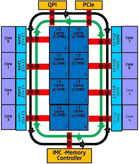
Figure 3: Ring Bus (Source: Intel)
As can be seen from the figure, the ring bus is actually two rings, one clockwise and one counterclockwise. All modules are equally connected to ring bus through ring stop. This design brings many advantages:
1) The double-ring design can ensure that the distance between any two ring stops does not exceed half of the total number of ring stops, and the delay is low.
2) The interaction between various modules is convenient, even no core. In this way, some advanced acceleration technologies, such as DCA (direct cache access), crystal beach, etc., came into being.
3) The high-speed ring bus ensures a great improvement in performance. Core to core latency is only about 60ns, while the bandwidth is as high as hundreds of Gb.
4) Convenient and flexible. To add a core, just add a new ring stop on the ring, and you don’t need to consider complicated interconnection issues as before.
Also according to Moore's Law, the performance of the ring bus will seriously decrease as the number of cores increases, and the overall delay of the system will be seriously affected after there are more than 12 cores. So a new variant is necessary:
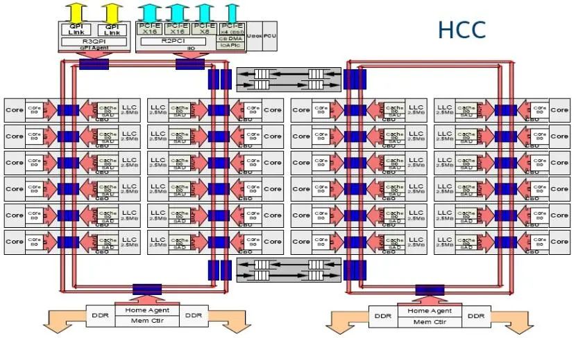
Figure 4: Xeon E5 v5 Platform (Source: Intel)
In the Xeon HCC (high core count) version, a ring bus is added. Each of the two ring buses is connected to 12 Cores to keep the delay within a controllable range. They are directly connected with two bidirectional pipe lines to ensure smooth communication. At the same time, because the module in Ring 0 accesses the module in Ring 1, the delay is significantly higher than that of the original ring, and the affinity is different, so the two rings belong to different NUMA (non-uniform memory access architecture) nodes. And special attention should be paid to this point in BIOS design.
At this time, there is another question. What if there are more cores than 12 and fewer than 24? Is it just stuffed into the first ring and pulled down? In fact, there is also a special design of 1.5 ring:
The one on the right is Xeon's LCC (low core count), which has only a single ring, while the MCC (middle core count) on the left is a half-ring design.
The problem is still happening. The transistors brought by Moore's Law are more used to increase the core rather than the speed (why does the frequency of the CPU stop at 4G? Have we reached the frequency ceiling?) The Xeon with 24 cores is far from the end, so what about more cores? Three rings design? how are they interconnected? These difficulties prompted Intel to find a new way.
Mesh Interconnect
Later, Intel introduced a new on-chip bus in Skylake and Knight Landing: Mesh. It is a 2D mesh network:
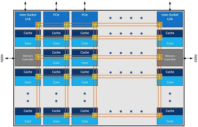
Figure 5: Intel Skylake-X and Skylake-Sp Utilize Mesh Architecture for Intra-Chip Communication (Source: Intel)
Mesh network has become more and more popular in recent years, and its flexibility has attracted more and more products to support it, including WiFi and other systems. The introduction of the on-chip bus in the Mesh network is a huge step, and it has many advantages:
1) Flexibility. It is very convenient to add new modules or nodes in Mesh. The delay it brings is not a linear increase like a ring bus, but a nonlinear one. Thus more cores can be accommodated. So there is no need to compromise on the 1.5 rings and 2 rings.
2) The two-way mesh network reduces the delay between two nodes. In the past, communication between two nodes had to bypass half of the ring at worst, but the distance between the overall nodes of the mesh is greatly reduced.
3) The external delay is greatly shortened:
a. RAM delay is greatly reduced.
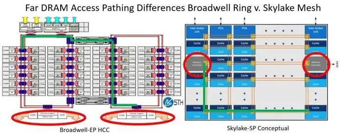
Figure 6: Far DRAM Access Pathing Differences Broadwell Ring v. Skylake Mesh (Source: Intel)
On the left is the ring bus, which accesses the memory controller in the other ring from one ring. In the worst case, the green line takes a big circle to reach the memory controller, and it takes 310 cycles. In the mesh network, the path is shortened a lot.
b. IO delay is reduced.
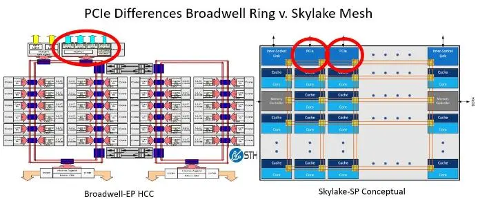
Figure 7: PCIe Differences Broadwell Ring v. Skylake Mesh (Source: Intel)
Mesh networks bring so many benefits, so what about the disadvantages? That's for sure, the added complexity of its gridded design has a negative impact on die size.

 English










