CMOS logic gate circuits are one of the most widely used circuits in ICs. It is composed of insulating field effect transistors. Since there is only carriers, it is a unipolar transistor integrated circuit. It is composed of PMOS and NMOS in a symmetrical and complementary form. This article first introduces the diode logic gate circuit, and then the CMOS gate circuit.
Diode Logic Gate
The unit circuit to realize basic logic operation and complex logic operation is called gate circuit or logic gate. And the gate circuit is the most basic logic unit in a digital integrated circuit. Commonly used gate circuits include: AND gate, OR gate, NOT gate, NAND gate, NOR gate, AND-NOR gate, XOR gate, etc. First understand the diode logic gate.
1. The AND Gate

(As long as one is low, the Y terminal will be pulled down to 0.7V)
The output high and low level values are not equal to the input values, and and the difference is equivalent to a voltage drop value. So this diode AND gate circuit is only used as a logic unit inside the integrated circuit, not use as the output to drive the load circuit.
2. The OR Gate
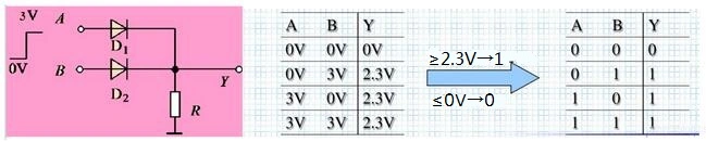
(As long as one is high, the Y terminal will be pulled up to 2.3V.)
3. Shortcomings
a. The output high and low level values are not equal to the input high and low levels, and the difference is a conduction voltage. If the output is used as the input signal of the next stage gate, high and low level shifts will occur.
b. The output end is connected to the load resistor to the ground, and the change of the resistance will affect the output high level. Therefore, this circuit is only used as a logic unit inside the IC, not an output.
CMOS Logic Gate
1. The NOT Gate
The CMOS inverter is the core of almost all digital integrated circuit designs. It has the advantages of large noise margin, high input resistance, low static power consumption, and insensitivity to noise and interference.
The CMOS inverter circuit consists of two enhanced MOSFETs, where NMOS for ground and PMOS for power. To make the circuit work normally, the power supply voltage VDD is required to be greater than the sum of the absolute values of the turn-on voltages of the two tubes.
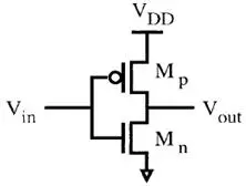
Figure 1: Inverter Structure
2. Commonly Used Logic Gates: NOR Gate, NAND Gate
In addition to the NOT gates, NOR gates, NAND gates, OR gates, AND gates, NOR gates, XOR gates, etc. are more commonly used.
The logical expressions are:
Y=(AB)’
T=(A+B)’
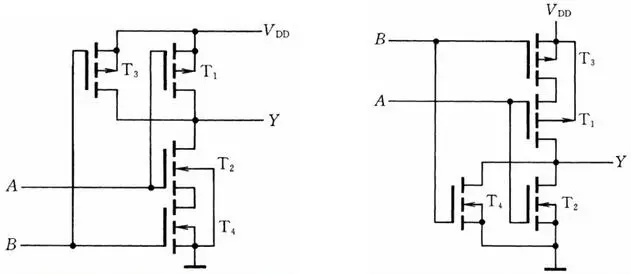
Figure 2: CMOS Logic Gate Circuits
The following mainly understands the disadvantages of the NAND gate and the improved circuits:
1) The output resistance R0 is affected by the input state, that is, the output resistance is different, and the difference can be four times, such as:
A=1, B=1,then R0 = Ron2 + Ron4 = 2Ron
A=0, B=0,then R0 = Ron2 // Ron4 = 1/2Ron
A=0, B=1,then R0 = Ron1 = Ron
A=0, B=0,then R0 = Ron3 = Ron
2) The high and low levels of the output are affected by the number of input terminals.
a. The more input ends, the more drive tubes are connected in series; the higher the output VOL, and the higher the VOH.
b. When all the input terminals are at low level, the more the input terminals are, the more loads are connected in parallel, and the output high level VOH is also higher.
3) When the Vgs of T2 and T4 reach the turn-on voltage, the corresponding Vi will be different.
 Which is faster, the NAND gate or the NOR gate with the same CMOS area?
In electronics, the mobility of electrons is 2.5 times that of holes (silicon-based). The calculation is to use these MOS tubes to drive the load capacitance of the subsequent stage. The flipping speed is related to the size of the load and the drive capability of the first stage. In order to have the same delay, PMOS needs to be more than twice the size of NMOS. As for the mobility of carriers, for PMOS, the carriers are holes; for NMOS, the carriers are electrons. So PMOS uses hole conduction, and NMOS uses electron conduction. Since the carrier mobility of PMOS is smaller than that of NMOS, the charging time of PMOS is longer than that of NMOS under the same size conditions.
In a complementary CMOS circuit, the NAND gate is connected in parallel with the PMOS transistors, and the NMOS transistors are connected in series, while the NOR gate is just the opposite. Therefore, under the same size condition, the speed of the NAND gate is fast. In short, in the complementary CMOS circuit, the AND gate is preferred.
To improve the above problems:
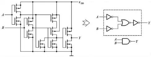
Figure 3: Improved Circuit Example
Use a NOR gate plus an inverter (the buffer is the NAND gate, as shown in the figure above.).
With a buffered gate circuit, the output resistance, output levels, and voltage transfer characteristics will not be affected by the state of the input terminal.
3. The OD Gate (open-drain)
OD gate: In order to meet the conversion of output level, absorb large load current and line and logic, change MOS to open drain.
The NAND gate structure diagram of OD output is as follows:
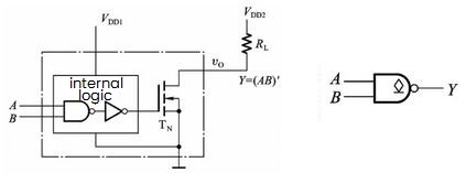
Figure 4: The NAND Gate Structure Diagram of OD Output
The OD gate work must be connected to the pull-up resistor RL to the power supply.
Application of OD gate: Multiple OD gate outputs can be directly connected to realize line-and logic, that is, the outputs are used in parallel, and line-and-or can be used for level conversion and driving. As shown below:
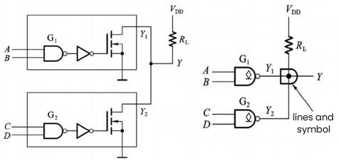
Figure 5: The OD Gate Circuit Application
Any one of Y1 and Y2 is low level, the output is low level, and when it is high, the output is high level.
4. Transmission Gate
CMOS transmission gate: Use the complementary characteristics of PMOS and NMOS to connect as shown in Figure 6:
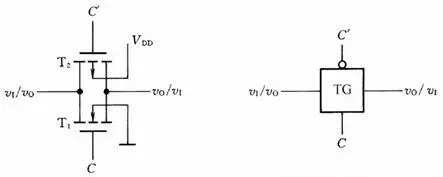
Figure 6: The CMOS Transmission Gate
T1 is an N-channel enhanced MOS transistor, and T2 is a P-channel enhanced MOS transistor. The source and drain of T1 and T2 are respectively connected as the input end and output end of the transmission gate.
C and C' are complementary control signals.
Since the structure of the CMOS transmission gate is symmetrical, the output end and the input end can be interchanged, and CMOS is a bidirectional device.
Applications:
1) The transmission gate and the inverter constitute an exclusive OR gate circuit:
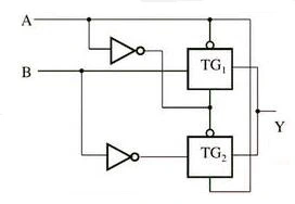
Figure 7: An Exclusive OR Gate Circuit
A=1, B=0, TG1 is off,TG2 is on,Y=B’=1
A=0, B=1, TG1 is on,TG2 is off,Y=B=1
A=0, B=0, TG1 is on,TG2 is off,Y=B=0
A=1, B=1, TG1 is off,TG2 is on,Y=B’=0
2) Analog switch:
Composed of transmission gates and an inverter.
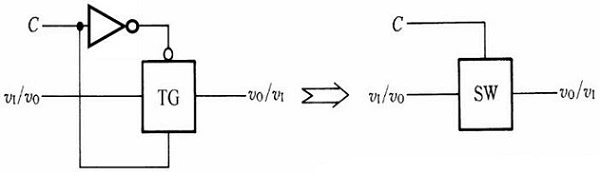
Figure 8: Analog Switching Circuit
Transmits continuously varying analog voltage signals.
5. Three-state Gate
1) High resistance state
This is an output state of the circuit, which is neither high nor low. If the high-impedance state is input to the next-level circuit, it will have no effect on the lower-level circuit. It can be understood as an open circuit and is not driven by anything.
Three-state gates are commonly used at the output of ICs, also known as output buffers.
2) The following figure is the structure of a CMOS three-state output inverter:
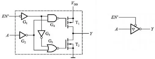
Figure 9: The Structure of a CMOS Three-state Output Inverter
When EN'=0, Y=A':
A=1, the output of G4 and G5 is high level, T1 is off, T2 is on, Y=0
A=0, the output of G4 and G5 is low level, T1 is on, T2 is off, Y=1
When EN’=1, regardless of whether A is high or low, G4 outputs high level, G5 outputs low level, T1 and T2 are off at the same time, and the output presents a high-impedance state.
3) Applications
Figure 10: Reduce the number of wires between cells:
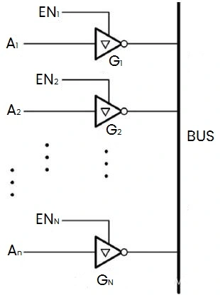
Figure 11: Bi-directional transmission of data
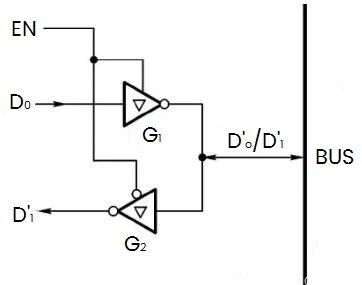
4) There are several common three-gate structures:
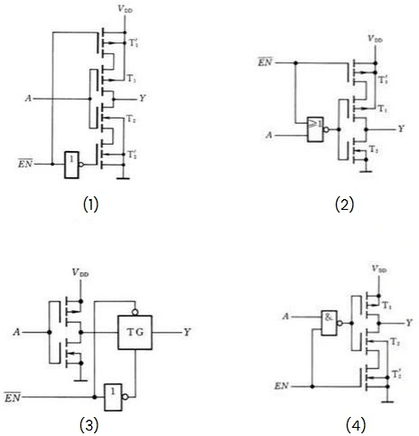
Figure 12: Common Three-gate Structures
(1) Three-state NOT gate: When ~ EN is 1, the top PMOS and bottom NMOS tubes are cut off, no matter what state A is, the output is in a high-impedance state, otherwise the output is Y= ~ A.
(2) Use a NAND gate to obtain a three-state buffer gate. When ~EN is high, the top PMOS transistor is cut off, and the output is in a high-impedance state, otherwise, the output is Y=A.
(3) Three-state NOT gate: Add a transmission gate after the inverter, when ~EN is low level, the transmission gate is turned on, and the output Y = ~A, otherwise the transmission gate is cut off, and the output is in a high-impedance state. If you want EN to be active at a high level, just swap the inverters at the upper and lower terminals of the transmission gate.
(4) Use a NAND gate to obtain a three-state buffer gate. When ~EN is high, the top PMOS tube is cut off, and the output is in a high-impedance state, otherwise the output is Y=A.

 English










