The memory hierarchy is the arrangement order of the storage systems under the computer architecture. Each layer has higher speed, lower latency, and smaller capacity than the next layer (with a few exceptions, such as AMD's early Duron CPUs). Most CPUs today are very fast, and most programs require memories access. And since cache efficiency and memory transfers are at different levels in the hierarchy, it can actually limit the speed of processing, causing the CPU to spend a amount of time waiting for data fetches. So how are the memories distributed? What are their characteristics?
Memory Hierarchy
The memory hierarchy in most computers is as follows:
1. Registers: Have the fastest access. For example, on a 32-bit processor, each register is 32 bits. The x86 processor has a total of 16 registers.
2. Cache (L1-L3: SRAM, L4: DRAM)
L1: Usually access only takes a few cycles, with dozens of KB.
L2: About 2 to 10 times higher latency than L1, usually hundreds of KB or more.
L3: Higher latency compared with L2, usually several MB in size.
L4 (not necessarily): DRAM outside the CPU, but the speed is higher than the main memory.
3. Main memory (DRAM): It takes hundreds of cycles to access and can be as large as tens of GB.
4. Disk storage: Thousands of cycles are required, and the capacity is very large.
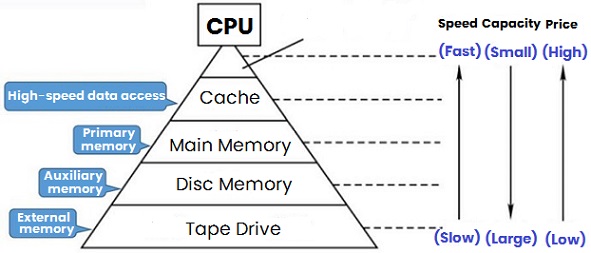
Figure 1: Computer Storage Hierarchy
Main Memory and Auxiliary Memory
There are many types of memory, which can be divided into main memory (referred to as primary memory) and auxiliary memory (referred to as secondary memory).
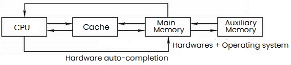
Figure 2: Main Memory and Auxiliary Memory
1) The most prominent feature of the primary memory is its fast access speed, so it is mainly used to store programs and data that will be used immediately. But its capacity is small and price is high.
2) The secondary memory is characterized by large capacity and low price, but slow access speed; it is mainly used to store temporarily unused programs and data.
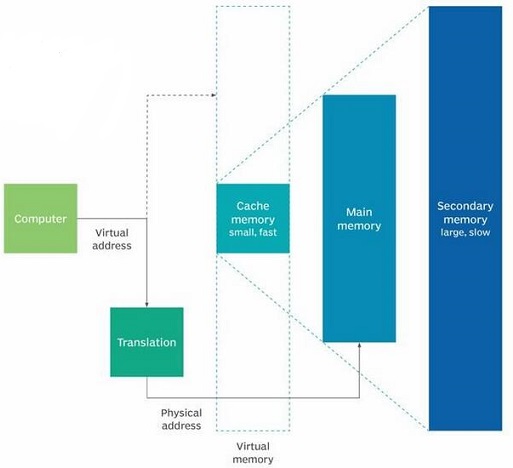
Figure 3: Memory Hierarchy in Computer System
Primary Memory
Memory plays a pivotal role in a computer. It generally uses semiconductor storage units, including random access memory (RAM), read-only memory (ROM), and high-speed CACHE.
Memory can be divided into two types: volatile memory and non-volatile memory. The former will lose data after power failure, and the latter can retain data even if the power off.
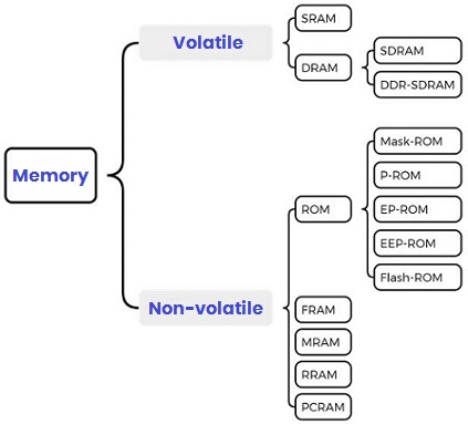
Figure 4: Types of Computer Memory
1. RAM
RAM is an internal memory that directly exchanges data with the CPU, also called main memory. It is a volatile memory, and is mainly used to store short-term use programs.
The reason why it is called "random access memory" is because it is compared to the early storage media. Because disc access is linear, the access time is determined by the distance between the tape location and the destination. It is necessary to turn the magnetic head to the proper position, so the longer the distance, the longer the reading and writing time. The latter RAM does not have this limitation, its access time is a fixed value, and the read time will not be affected by the location of the stored data in the memory.
RAM can be roughly divided into two types:
SRAM (Static RAM), used for Cache
DRAM (Dynamic RAM), used for main memory
The basic principles of the two are the same, both store the charge in the memory, thus storing 0 or 1 for different charges. The following is a summary of the characteristics of both:
|
Specifications
|
SRAM
|
DRAM
|
|
Store information
|
Trigger
|
Capacitor
|
|
Destructive read
|
No
|
Yes
|
|
Rewrite after reading
|
No
|
Yes
|
|
Running speed
|
Fast
|
Slow
|
|
Integration
|
Low
|
High
|
|
Heat
|
More
|
Less
|
|
Cost
|
High
|
Low
|
|
Refresh
|
No
|
Yes
|
|
Run column address
|
Once
|
Twice
|
Except that, the structure of SRAM is more complex, the capacity per unit area is small, and the access speed is very fast. Whine the structure of DRAM is simple, the storage capacity per unit area is relatively large, and the access time is slower than that of SRAM. It is relatively simple. The DRAM stored charge will gradually disappear over time, so regular refresh is required to maintain the data stored in the capacitor.
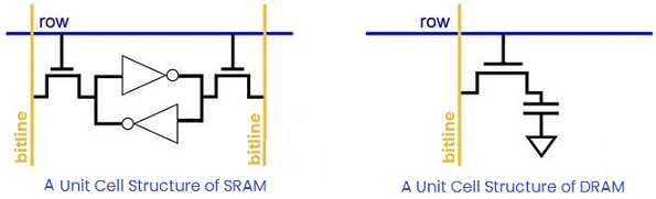
Figure 5: Storage Structure
It can be seen from the structure of SRAM and DRAM in the figure that SRAM uses positive and negative transistors + capacitors (flip-flop) to construct memory, and DRAM just uses capacitor storage. Due to the different characteristics of them, SRAM is more powerful as a Cache for fast access by the CPU, while DRAM is more suitable as a main memory.
2. ROM
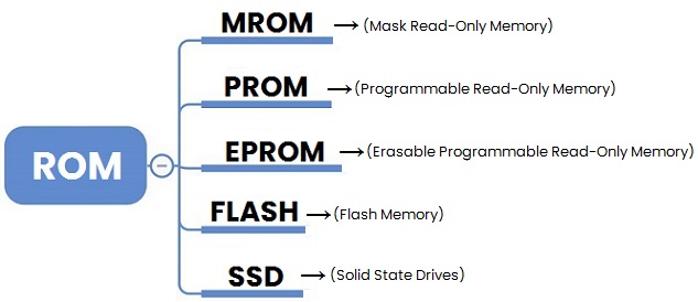
Figure 6: ROM Types
When ROM is manufactured, information (data or programs) is stored and permanently stored. These information is read-only, even if the device power off, the data will not be lost. ROM is generally used to store the basic programs and data of the computer, such as BIOS ROM. Its physical shape is generally a dual in-line (DIP) package.
Generally speaking, ROM is developed under the disadvantages of RAM. Later, it was discovered that the programs in the ROM sometimes needed to be modified, so new memories were developed, such as EPROM, EEPROM, Flash, etc.
Nowadays, it is no longer possible to simply refer to a memory as RAM or ROM. The characteristics of each memory are crossed.
At present, ROM has basically adopted EEPROM and Flash ROM as storage media. Commonly used FLASH memories mainly include NAND Flash and NOR Flash. They differ in internal structure, performance and applications.
RAM vs ROM
Generally speaking, it is difficult to understand the relationship between RAM and ROM and the running memory and hard disk capacity. In fact, they are the same in a general sense, but there are some differences from the perspective of computers and mobile phones.
It is generally easier to understand from the perspective of computers. RAM is what we usually call running memory, and it is indeed readable and writable at any time. Because the data processed by the CPU is mediated by the running memory, the data is not saved after power off.
Compared with RAM and ROM, the biggest difference between the two is that the data stored on RAM will disappear automatically after power off, while on ROM will not disappear automatically and can be saved after power off for a long time.
3. FLASH Memory
NAND Flash
NAND means Not AND (NAND gate), which means that the basic unit of the Flash is a NAND gate, as shown below:
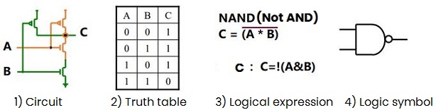
Figure 7: Not AND
1) Structure: NAND flash adopts a parallel structure and organizes storage cells into storage cell arrays. Each cell contains multiple pages, each page contains multiple blocks, and each block contains multiple sectors. This structure has higher storage density.
2) Features:
High storage density: Usually higher than that of NOR Flash, which is suitable for storing large-capacity data.
Fast reading speed: It is suitable for applications that read a large amount of data quickly.
Long erasing and writing time: Erasing operations are usually done in units of blocks.
Suitable for storage applications: Due to high storage density and low cost, NAND flash is widely used in mass storage devices, such as solid state drives (SSDs), USB drives and memory cards.
NOR Flash
Nor means Not OR (NOR gate), which means that the basic unit of the Flash is the NOR gate, as shown below:
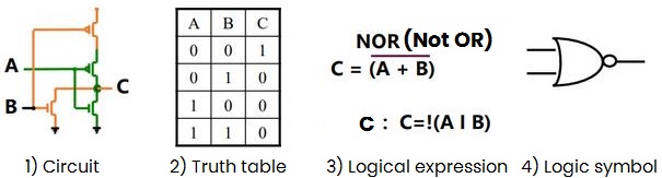
Figure 8: Not OR
1) Structure: NOR Flash memory adopts a parallel structure, and organizes storage cells into storage cell arrays. Each cell array contains multiple blocks, and each block contains multiple sectors. This structure has a faster reading speed and lower access latency.
2) Features:
Fast read speed: NOR Flash is suitable for applications that require fast random access.
Erase and write operations are faster: The Flash can be erased by byte or by sector.
Low storage density: It is suitable for storing small-capacity codes and programs.
Code execution: Due to its fast reading speed and random access capability, NOR Flash is widely used in embedded systems to store code, firmware and startup programs, etc.
Both Flash ROM (Flash Read-Only Memory) and EEPROM (Electrically Erasable Programmable Read-Only Memory) are non-volatile memories, but there are some differences in their working principles and applications.
|
Characteristics
|
Flash ROM
|
EEPROM
|
|
Erase and program
|
Long erasing time and slow erasing speed, and program operations can be performed on single byte or smaller memory cells.
|
Short erasing time and fast erasing speed. It can be erased and programmed in bytes, which are more flexible and fine-grained.
|
|
Storage density
|
High storage density and can hold a large amount of data. This makes it useful for storing large volumes of programs, firmware, and data.
|
Low storage density, and it is usually suitable for storing small amounts of data, such as configuration information, user data, etc.
|
|
Applications
|
Widely used in firmware storage, BIOS storage, fixed data storage and other applications that require large capacity and fast access.
|
Often used to store small-capacity information, calibration data, user settings, and other data that require frequent modification and maintenance.
|
4. Cache
Cache is located between the CPU and the main memory, with a faster read and write speed than the memory. When the CPU writes or reads data into memory, this data is also stored in cache memory. If the CPU needs the data again, the CPU reads the data from the cache memory instead of the memory. Of course, if the required data is not in the cache, the CPU will read the data in the memory again.
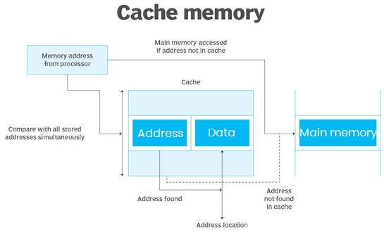
Figure 9: Cache Memory
In the mobile phone, RAM is the same as the running memory of the computer; and the ROM is hooked up to the hard disk. Part of the ROM in the mobile phone is used to store system information and some installed software. Most of the remaining capacity is just to use as a hard disk, readable and writable.
Secondary / Auxiliary Memory
The data needs to be loaded from the auxiliary memory into the memory before it can be read and processed by the CPU.
The difference between primary memory and secondary memory is huge, mainly including:
|
Differences
|
Primary Memory
|
Secondary Memory
|
|
Access speed and latency
|
Fast access speed, the CPU can read or write data in a few nanoseconds. It has low latency and high bandwidth and is suitable for storing executing programs and temporary data.
|
Low access speed, usually measured in milliseconds. It has higher access latency and takes more time to read and write data.
|
|
Cost/Capacity
|
Expensive, due to its high speed and performance advantages, memory is an important part of computer systems, but its storage capacity is limited and its cost is high.
|
Relatively cheap, with larger storage capacity, which can hold a large amount of data and is suitable for long-term storage and data backup.
|
|
Persistence
|
Volatile, which means data in memory will lost when power off. The data in memory needs to be saved to secondary memory or other non-volatile storage media periodically to prevent data loss.
|
Non-volatile, even in the case of power failure, the data in the secondary memory can remain unchanged.
|
It should also be noted that since the CPU, memory, and I/O devices have been integrated into a small chip inside the microcontroller, its memory includes program memory (usually flash memory or EEPROM) and data memory (RAM). Program memory is used to store the code of the MCU, while data memory is used to store variables and data during program execution.
Computer Disk
1) The disk is composed of platters.
2) Each platter is composed of sectors one by one, and is divided into a group of concentric circles called tracks along the radial direction.
3) Each track is cut into many fan-shaped areas called sectors. Each is the smallest unit for reading and writing information from a disk and contains an equal number of data bits, usually 512 bytes.
4) A cylinder composed of tracks with the same radius on different platters is called a cylinder.
The capacity of the disk: the number of heads × the number of tracks × the number of sectors × the number of bytes per sector
Disc array is composed of many disk drives or CD drives according to certain rules, such as striping, declustering, interleaving, etc. to form a fast, large capacity external memory sub system.
Under the control and management of the array controller, disc memory realizes fast, parallel or interleaved access, and has strong fault tolerance. From the user's point of view, although a disk array is composed of several, dozens or even hundreds of disks, it can still be considered as a single disk, and its capacity can be as high as hundreds to thousands of gigabytes. And it widely used in multimedia systems.
Solid State Disk (SSD)
SSD consists of one or more flash memory chips and a flash translation layer.
1) Flash memory chip stores content.
2) The flash translation layer translates requests for logical blocks into accesses to underlying physical devices.
The storage unit is the core component of a hard disk, and choosing an SSD is actually choosing a storage particle. At present, according to the difference in density, flash memories are mainly divided into five types: SLC, MLC, TLC, QLC, and PLC (unavailable):
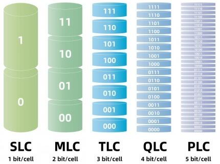
Figure 10: Types of NAND Flash Memory
SLC
The full name of SLC is Single-Level Cell, which is 1bit/cell. This also means that the SSD capacity using SLC is destined not to be too large, and other aspects of SLC are better than other types of flash memory particles.
Features: fast speed and long life, expensive (about 3 times the price of MLC), about 100,000 times of erasing and writing life.
The erasing and writing life of SLC is the longest among them, which can reach about 100,000 times. In addition, SLC has the fastest reading and writing speed, the most accurate reading and writing data, the best quality and the most expensive cost. At present, it is basically only used in enterprise-level high-end solid state drives, and there are very few high-end consumption grade SSD is in use.
MLC
The full name of MLC is Multi-Level Cell, which is 2bit/cell.
Features: high speed, long life, expensive, about 3000-10000 erasing and writing life. A little better than SLC, but the cost is much lower than SLC.
However, the erasing and writing life of MLC is much worse than that of SLC, which can only reach about 10,000 times. And compared with SLC, MLC's read and write speed, quality, and accuracy are all inferior to SLC. It is currently mostly used in industrial storage. However, with technology and consumption developed, there are also some brands that will use MLC to improve the level of consumer products.
TLC
The full name of TLC is Trinary-Level Cell, that is, 3bit/cell, and some Flash manufacturers call it 8LC.
Features: average speed, average lifespan, slightly more expensive, about 500-1000 erasing lifespan.
TLC is currently the most common flash memory particle. Although TLC's read and write speed, particle quality and lifespan are not as good as SLC and MLC, its cost is much lower. If it is used as a daily use, it can fully meet the needs of ordinary consumers. At present, TLC is mostly used in mid-to-high-end SSDs on the market, and is favored by mainstream SSDs.
QLC
The full name of QLC is Quad-Level Cell, which is 4bit/cell. Its erasing and writing life is the shortest, only up to 150 times, but it has the highest storage density and the lowest cost, so its advantages are obvious. At present, it is mainly used by low-end large-capacity SSDs, which can bring longer service life to large-capacity SSDs, and is enough for some consumers' daily use.
PLC
The full name of PLC is Penta-Level Cell, which is 5bit/cell. The flash memory granule has not yet been officially released, but it is expected to come out in the next few years. It is believed that it can bring larger storage space and lower cost of unit storage to SSD products. However, the promotion of PLC will be greatly limited by its speed and lifespan, and further understanding is needed.
Other Parameters
According to the above content, the flash memory particles can be sorted according to data stability, speed and price as SLC>MLC>TLC>QLC>PLC, and the capacity is opposite SLC Flash technology have achieved a leap in performance.
1. Storage capacity: number of storage words x storage word length (such as 1M x 8 bits).
MAR reflects the number of stored words, and MDR reflects the stored word length.
2. Unit cost: price per person = total cost/total capacity (For example, the price of a memory stick is $259, and the capacity is 8GB, then unit cost = 259 / (8*8) ).
3. Storage speed: data transfer rate = data width/storage cycle
4. Access time: access time + recovery time = access period, after the computer performs a read and write operation, it needs a period of recovery time before the next read and write operation can be performed.
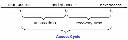
Figure 11: Memory Access Time
5. Bandwidth: It is the data transmission rate, which means the maximum amount of info entering and leaving the main memory per second, and the unit is word/s, byte/s, bit/s.
Units
The basic unit of computer storage capacity is byte, and the storage units are arranged in ascending order: B, KB, MB, GB, and TB. The conversion formula is as follows:
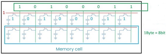
Figure 12: Memory Cell
1B=8bit, 1KB=1024B, 1MB=1024KB, 1GB=1024MB, 1TB=1024GB
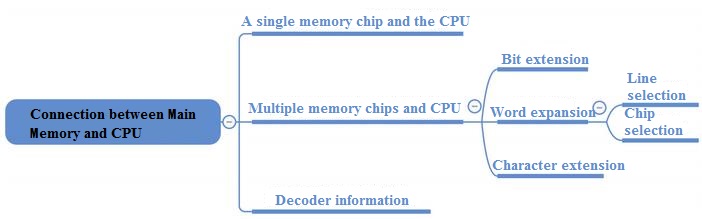
Connection between Main Memory and CPU
1. The connection between a single memory chip and the CPU.
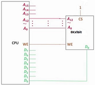
Suppose there is an 8Kx1-bit memory chip, which means that the chip needs 13 address lines, and the CPU has 8 data lines and 16 address lines. It can be seen from the above that the CPU can only transmit 1 bit of data to the chip at a time. This will cause the data line of the CPU to be underutilized, and there will be a situation where the main memory capacity needs to be expanded.
Therefore, it is necessary to do it by rationally connecting multiple memory chips. There are two ways:
2. Connection between multiple memory chips and CPU
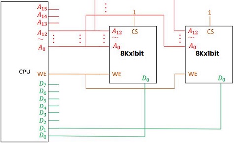
(1) Bit extension: expand the word length of the storage unit.
As shown in the figure above, when two memory chips are connected, the CPU address bus A0~A12 will be sent to the two chips together, and the data line D0 of the second chip will be connected to the data line D1 of the CPU. In this way, it is expanded into a memory of 8Kx2 bits.
Similarly, there are a total of D0~D7 data lines in the CPU, so a total of 8 memory chips shown in the figure can be connected to expand into 8Kx8-bit memory.
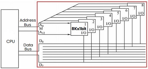
(2) Word expansion: expand the number of storage units.
The picture shows an 8Kx8-bit memory chip. Since the word length of the memory unit of the chip is equal to the number of data buses of the CPU, no bit expansion is required. The address lines are not fully utilized, so word expansion can be considered.
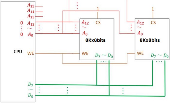
There are two types of word extensions:
Line selection method:
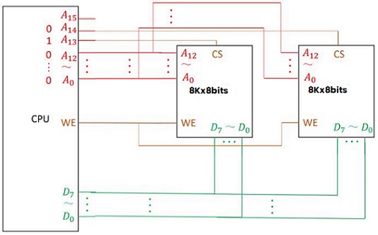
Use a special address line as a chip selection line to choose a certain memory chip.
As shown in the figure: A13 is the chip selection line of the first memory chip, and A14 is the chip selection line of the second memory chip. When A13 and A14 are respectively 01 or 10, it means that the first memory chip or the second memory chip is selected. So that the number of storage units can be expanded.
At this time, the lowest address of the first memory chip is: 01 0000 0000 0000, and the highest address is 01 1111 1111 1111.
The lowest address of the second memory chip is: 100 0000 0000 0000, and the highest address is 101 1111 1111 1111.
But this method has a flaw: A13 and A14 cannot take 00 or 11, because when taking 00, both memory chips will not be selected, and 11 will cause both memory chips to be selected, even n chip select signals are needed.
Optimization:
Selection is done only through A13 and a NOT gate.
At this time, the lowest address of the first chip is 10 0000 0000 0000, and the highest address is 11 1111 1111 1111.
The lowest address of the second chip is 00 0000 0000 0000 and the highest address is 01 1111 1111 1111.
Chip selection method:
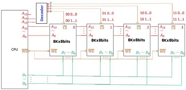
Summary:
|
Line Selection
|
Decode Chip Selection
|
|
n lines→n selection signals
|
n lines→2n selection signals
|
|
Simple circuit
|
Complex circuit
|
|
The address space is not contiguous.
|
The address space can be contiguous.
|

 English










