Advanced packaging is a product of semiconductor development. In electronics, packaging is the technology of assembling integrated circuits into chips as final products. It is an important part of the electronics industry, which affects the performance, reliability and lifespan of electronic components. As chip technology develops, so does packaging technology.
The most basic function of packaging is to protect the chips affected by the surroundings. Therefore, in the original microelectronic packaging, the metal can was used as the casing, and the fragile electronic components were protected by a completely isolated and airtight method from the outside. However, with the development of integrated circuit technology, especially the continuous improvement of chip layers technology, the function of packaging is also gradually alienated. Here several mainstream packaging technologies are introduced below.
Main IC Packages Introduction
Flip-Chip
Flip-Chip was first proposed in the 1960s. Compared with the wire bonding of the traditional package, it adopts Bump, RDL and other connection methods, which overcomes the problem of the limit of the center distance of the wire bonding pad, and has the advantages of shortening the interconnection length, excellent thermal performance, and high reliability.
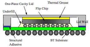
Figure 1: Flip-Chip Package
Flip-chip packaging is a leadless structure that generally contains circuit units. Designed to be electrically and mechanically connected to a circuit by an appropriate number of solder balls on its face. During the process, deposit tin-lead balls on the I/O pad, then turn the chip over to heat, and combine the molten tin-lead balls with the ceramic substrate. This technology replaces conventional wire bonding and has gradually become the mainstream of packaging. Currently, it is mainly used in high-frequency CPUs, GPUs and Chipset and other products. Compared with COB, the chip structure and I/O terminals (solder balls) of this packaging are facing downward. Since the I/O terminals are distributed on the entire chip surface, Flip chip has reached its peak in terms of packaging density and speed. In particular, it can be processed by means similar to SMT technology, so it is a good direction of chip packaging technology and high-density installation. There are three main types of flip chip connection: C4 (Controlled Collapse Chip Connection), DCA (Direct Chip Attach) and FCAA (Flip Chip Adhesive Attachment).
The thermal performance of Flip-Chip packaging is obviously superior to the conventional wire bonding process, which is determined by its low thermal resistance heat sink and structure. Another important advantage of it is electrical performance. Many electronic devices today operate at high frequencies, so signal integrity is very important. In the past, 2-3GHZ was the upper frequency limit for IC packages, and using flip-chip packages could reach 10-40GHZ with a better substrate technology.
FOWLP (Fan-Out Wafer Level Packaging)
FIWLP is mainly used in chips with small area and few pins. As the number of pins increases, the Fan-out WLP packaging form is derived, that is FOWLP.
Before the emergence of WLP technology, the traditional packaging process steps were mainly carried out after the die was cut and sliced. That is, dicing first, and then packaging into various forms.
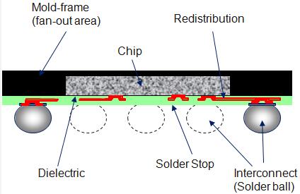
Figure 2: FOWLP (source from Wikipedia)
WLP has two types: Fan-in and Fan-Out. It is different from traditional packaging. Because most of packaging processes is on the wafer, and then have dicing after the packaging is completed. Under this, the size of the packaged chip is almost the same as that of the die, so it is also called CSP (Chip Scale Package) or WLCSP (Wafer Level Chip Scale Packaging). The advantages of WLP are light, small, short and thin.
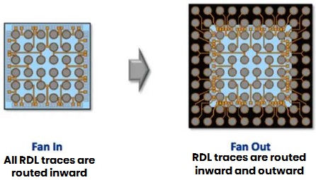
Figure 3: Fan In and Fan Out
At the beginning, WLP mostly adopts the Fan-in type, which can be called Fan-in WLP or FIWLP, and is mainly used in chips with a small area and few pins. With the improvement of IC technology, the chip area shrinks, and the chip area cannot accommodate enough pins. Therefore, FOWLP came out to make full use of RDL for connections outside the chip area to get more pins.
It needs to lead RDL and Bump to the periphery of the die, so it is necessary to first dicing and dividing the wafer, and then reconfigure the independent pieces into the wafer process, and based on this, through batch processing, metal wiring to form the final package.
No matter Fan-in or Fan-out, the connection between WLP package and PCB is in the form of flip chip, and the active side of the chip is facing down to the printed circuit board, which can realize the shortest electrical path, and also ensures for higher speeds and fewer parasitic effects. On the other hand, due to the batch packaging, the entire wafer can be packaged at one time, and the cost reduction is another driving force for wafer-level packaging.
The main manufacturer is Infineon and NXP, which is mainly used in the fields of mobile phones, 5G, and AI.
InFO (Integrated Fan-Out)
In 2016, the InFO technology was developed by TSMC. It is the integration of the FOWLP, which can be understood as the integration of multiple chips based on FOWLP. InFO provides space for multiple chip integration, and can be used for radio frequency and wireless chips, processor and baseband chip packaging, graphics processor and network chips.
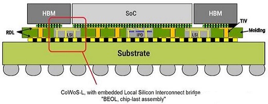
Figure 4: TSMC InFO Package
With the large-scale application of InFO technology and the further development of embedded WLB technology, a number of new manufacturers and FOWLP technology may enter the market. When TSMC announced that InFO technology was ready for mass production in 2014, the RDL pitch was smaller (such as 10 microns), and the thickness of the package was thinner.
InFO gives more options, such as 8mm x 8mm platform for RF and wireless chip packaging, 15mm x 15mm for application processor and base-band chip packaging, and larger sizes such as 25mm x 25mm for GPUs and other networking applications.
FOPLP (Fan-out Panel Level Package)
In 2017, the FOPLP was developed by Samsung. It is also an extension of FOWLP, and is mainly used in mobile devices, 5G, and AI fields. FOPLP carries out the Fan-Out process on a larger square substrate, which can be a PCB or a glass used for LCD. At present, FOPLP uses a 24×18 inch (610×457mm) PCB board, whose area is about 4 times that of a 300mm silicon wafer. And it can integrate the front and rear processes of packaging, which can be regarded as a one-time packaging process, so it can greatly reduce costs.
FOPLP adopts the production technology on the PCB to produce RDL. Its line spacing are currently greater than 10um. And SMT equipment is used to mount chips and passive components. Since its panel area is much larger than the wafer area, it can be processed at one time with more products.
EMIB (Embedded Multi-Die Interconnect Bridge)
EMIB technology developed by Intel in 2018 belongs to substrate-based packaging. Its concept is similar to the 2.5D package based on the silicon interposer, which is to perform local high-density interconnection through the silicon chip. In addition, there is no TSV, EMIB has the advantages of normal package yield, and simple design processes.
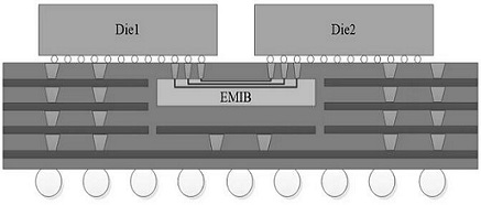
Figure 5: Embedded Multi-Die Interconnect Bridge
For traditional SoC chips, CPU, GPU, memory controller and IO controller can only be manufactured using one process. While using EMIB technology, the CPU and GPU have high requirements on the process, and can use 10nm process, IO unit and communication units can use 14nm process, and the memory part can use 22nm process. That is, EMIB can integrate three different processes into one a processor.
For example, the KBL-G platform integrates the Intel Core processor and the AMD Radeon RX Vega M GPU, such chip has the powerful computing power of the Intel processor and the excellent graphics capability of the AMD GPU, and also has an excellent cooling experience. It made history and brought the consumer experience to a new level.
CoWoS
CoWoS, the 2.5D packaging technology launched by TSMC in 2012 is to package chips on a silicon interposer, interconnect them using high-density wiring on the silicon interposer, and then install them on the packaging substrate. This technology achieves the effects of small package size, high performance, low power consumption, and fewer pins.
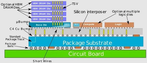
Figure 6: TSMC CoWoS
Both CoWoS and InFO come from TSMC, CoWoS has silicon interposer, but InFO does not. Because CoWoS is aimed at the high-end market, and the number of connections and package size are relatively large, while InFO is aimed at the cost-effective market, the package size is small, and the number of connections is relatively small.
CoWoS products are mainly used in the production of high-end servers, high-end enterprise applications, high-performance computing and other fields. TSMC says the 5th generation products has 20 times the number of transistors compared to the 3rd generation. The new packaging technology increases the interposer area by 3 times, uses a new TSV solution, and has thicker copper connection lines. At present, this technology has been used to manufacture AMD MI200 "Aldebaran" professional computing card, which encapsulates 2 GPU cores and 8 HBM2e caches.
TSMC also said that the new technology also uses a better heat conduction method. The 5th gen technology uses metal heat conduction materials, and the thermal resistance is reduced to 0.15 times that of the previous one, which is helpful for such high-performance chips. The company is still developing the sixth-gen solution to integrate more chiplets and DRAM chips. It is expected that two computing chips and eight or more HBM3 DRAM chips can be accommodated in the same package.
HBM (High-Bandwidth Memory)
HBM is mainly aimed at the high-end GPUs. It uses 3D TSV and 2.5D TSV technologies to stack multiple memory chips together through 3DTSV and 2.5D TSV technology to interconnect the stacked memory chips and GPU on the carrier board.
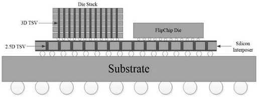
Figure 7: High-Bandwidth Memory
The main application manufacturers are AMD, Nvidia, Hynix, Intel, and Samsung, and their products are mainly used in the fields of image processing and high-performance computing.
HBM currently has three versions, HBM, HBM2, and HBM2E, with bandwidths of 128GBps/Stack, 256GBps/Stack, and 307GBps/Stack, respectively. On 20 October 2021, SK Hynix said that it has finished development of HBM3 memory devices.
The HBM standard was promoted by AMD, NVIDIA and Hynix. AMD first used the HBM standard in its flagship graphics card, with a memory bandwidth of up to 512GBps, and then NVIDIA used the HBM standard to achieve a memory bandwidth of 1TBps. Compared with DDR5, the performance of HBM has been improved by more than 3 times, and the power consumption has been reduced by 50%.
HMC (Hybrid Memory Cube)
The HMC standard pushed by Micron, uses stacked DRAM chips to achieve greater memory bandwidth. In addition, HMC integrates the memory controller into the DRAM stack package through 3D TSV technology. In the past, the memory controller was built in the processor, so in high-end servers, when a large number of memory modules need to be used, the design of the memory controller is very complicated. Now that it is integrated into the memory module, the design is greatly simplified. In addition, HMC uses a high-speed serial interface (SerDes), which is suitable for situations where the processor and memory are far away.
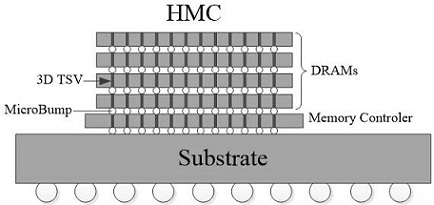
Figure 8: Hybrid Memory Cube
Comparing HBM and HMC, it can be seen that the two are very similar. They both stack DRAM chips and interconnect them through 3D TSV, and there are logic control chips underneath them. The difference between the two is: HBM is interconnected through interposer and GPU, while HMC is directly installed on substrate, without interposer and 2.5D TSV in the middle.
In the HMC stack, the diameter of 3D TSV is about 5~6um, and the number exceeds 2000+. DRAM chips are usually thinned to 50um, and the chips are connected by 20um MicroBump.
The main manufacturers are Micron, Samsung, IBM, ARM, and Microsoft, and their products are widely used in the production of high-end servers, enterprise applications, and high-performance computing.
Wide-I/O (Wide Input Output)
Wide-I/O is a broadband input technology mainly promoted by Samsung. It is realized by stacking the memory chip on the logic chip through 3D TSV. At present, it has developed to the second gen, which can realize a memory interface bit width of up to 512bit, a memory interface operating frequency of up to 1GHz, and a total memory bandwidth of up to 68GBps, which is twice of the DDR4 interface.
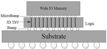
Figure 9: Wide Input Output
This technology has the advantages of vertical stack packaging of TSV architecture, which helps to create mobile memory with speed, capacity and power characteristics, and meets the needs of mobile devices such as smart phones, tablet PCs, and handheld game consoles. So its main target market is mobile devices requiring low power consumption.
Foveros
Foveros is a high-performance 3D face to face chip stack for heterogeneous integration packaging technology is promoted by Intel. Compared with 2D EMIB, it is more suitable for small-sized products or products with higher requirements on memory bandwidth, and it also has advantages in size and power consumption. In addition, the power of the data it transmits per bit is very low, and its technology has to deal with the reduction of bump pitch, the increase of density and the chip stacking.
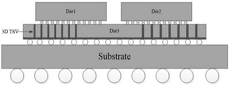
Figure 10: Foveros 3D
The first Foveros 3D stacking designed motherboard chip, LakeField, integrates a 10nm Ice Lake processor and a 22nm core. It has complete PC functions, but its size is only the size of a coin.
Although Foveros is a more advanced 3D packaging technology, it is not a substitute for EMIB. Intel will use the two in combination in subsequent manufacturing. The difference between EMIB and Foveros is that the former is a 2D packaging technology, while the latter is a 3D stacked packaging. Compared with the 2D EMIB, Foveros is more suitable for small-sized products or products that require higher memory bandwidth. In fact, there is not much difference between the two in terms of chip performance and functions. However, in terms of size, power consumption, etc., Foveros is better.
Co-EMIB
CO-EMIB is a combination of EMIB and Foveros. EMIB is mainly responsible for the horizontal connection, allowing chips with different cores to be spliced together like a puzzle, while Foveros is vertical stacking. Therefore, Co-EMIB is a more flexible chip manufacturing method, which allows chips to be stacked while continuing to be spliced horizontally to create a larger chip system. So it is a better way to maintain and continue the existing computing architecture and ecology.
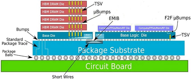
Figure 11: Intel Introduces Co-EMIB
Co-EMIB packaging can provide performance comparable to that of a single chip. The key to achieving this technology is ODI (Omni-Directional Interconnect) technology. ODI has two different types. In addition to the elevator connection of different floors, there are also sky bridges connecting different 3D structures and mezzanines between floors, allowing different chip combinations to have extremely high flexibility. Co-EMIB uses a brand-new 3D + 2D packaging method to change chip design from a flat puzzle in the past to a stacking block.
SoIC (System-on-Integrated-Chips)
SoIC is an innovative multi-chip stacking technology proposed by TSMC, which can integrate wafer-level processes below 10nm. The most distinctive feature of this technology is the bonding structure without bumps, so it has higher integration density and better operating performance.
SoIC includes two technical forms of CoW (Chip-on-wafer) and WoW (Wafer-on-wafer). It is a kind of WoW or CoW direct bonding technology belongs to Front-End 3D technology (FE 3D), while the InFO and CoWoS mentioned above belong to Back-End 3D technology (BE 3D). And TSMC and Siemens EDA (Mentor) cooperated on SoIC technology and launched related design and verification tools.
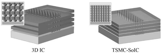
Figure 12: 3D IC and SoIC
Specifically, the manufacturing process of SoIC and 3D IC is somewhat similar. The key of SoIC is to realize the junction structure without bumps, and its TSV density is higher than that of traditional 3D IC. It can directly realize multiple chips through extremely tiny TSV between layer chips. The above figure shows the comparison of TSV density and bump size between the two. It can be seen that the TSV density of SoIC is much higher than that of 3D IC.
X-Cube (Xtended-Cube)
The X-Cube 3D packaged chips are connected by TSV technology, which reduces power consumption while increasing the transmission rate, and greatly shortens the signal transmission distance between chips, and can also customize memory bandwidth and density according to needs.
For the interconnection between dies, it uses the TSV technique. At present, Samsung's own X-Cube test chip has been able to stack the SRAM layer on top of the logic layer with their own 7nm EUV process. This way can separate the SRAM from the logic part, making it easier to expand the capacity.
X-Cube can be flexibly applied to future chips, including 5G, AI and high-performance computing fields. At present, the technology can already support 7nm and 5nm processes.
In May 2021, Samsung announced that the next-generation 2.5D Interposer-Cube4 (I-Cube4) will be available soon, which can use a silicon interposer for one or more logic chips and multiple high-bandwidth memory chips, so the chips are arranged and packaged in one chip.
In November 2021, Samsung has launched a new 2.5D H-Cube (Hybrid Substrate Cube), dedicated to HPC, AI, data centers and network products that require high performance and large packaging areas.

 English










