A low dropout regulator (LDO) is a voltage stabilizer used to adjust and control voltage difference in circuits. LDOs are distinguished by their ability to maintain regulation with small differences between supply voltage and load voltage. They can provide a relatively constant output voltage regardless of changes in input voltage. Because of their unique characteristics, they are popular in analog and digital systems.
Low-Dropout Regulators (LDOs)
Basic Info
The working principle of LDO is based on negative feedback control technology. When the input voltage changes, the error amplifier detects it in the output voltage and compares it to the reference voltage. If the output voltage is lower than the set value, the error amplifier will adjust the power transfer element to increase the output voltage, on the contrary, it will play a role to decrease the output voltage. That is, by continuously adjusting the power delivery components, the voltage regulator maintains the output voltage within a constant range.
A low dropout regulator usually consists of three main parts: a reference voltage source, an error amplifier, and a power transfer element. The reference voltage source generates a stable base voltage, and the error amplifier monitors the difference between the output voltage and the reference voltage and feeds it back to the power transfer element to adjust the output voltage.
In other words, LDOs usually use a series amplifier structure composed of diodes and transistors. This can provide high gain and low output impedance, thereby achieving better voltage regulation. In addition, the voltage regulator may also include features such as overcurrent protection, short circuit protection, and overtemperature protection to ensure safe operation of the circuit.
Main Parameters
The performance of a LDO is described by a series of specifications. Here are some common specifications:
1) Input voltage range: Refer to official data and manuals.
2) Output voltage range: Refer to official data and manuals.
3) Load regulation: The degree of fluctuation of the output voltage when the load changes. And lower load regulation indicates better stability.
4) Line regulation: The degree of fluctuation of the output voltage when the input voltage changes. And a lower value indicates greater response to changes in input voltage.
5) Dropout voltage: The minimum difference between the input voltage and the output voltage. And a lower value means that the regulator can operate at a lower input voltage and provide a stable output voltage.
6) Load capacity: The maximum current that the voltage regulator can provide to the load. And it determines the load type and load current range that the regulator can support.
7) Temperature coefficient: The degree to which the output voltage changes with the ambient temperature. And a lower value means the regulator is less affected by temperature changes.
8) Output noise: The stray noise present in the output voltage of the voltage regulator, the smaller the better.
9) Protection: Include over-current protection, short-circuit protection, over-temperature protection and other functions to protect the circuit from unexpected damage.
In short, LDO is an important electronic component used to provide stable DC power supply. When selecting it, its specifications, such as input voltage range, output voltage range, load regulation, etc., need to be considered to meet system requirements and ensure stable operation of the circuits.
TO252-3
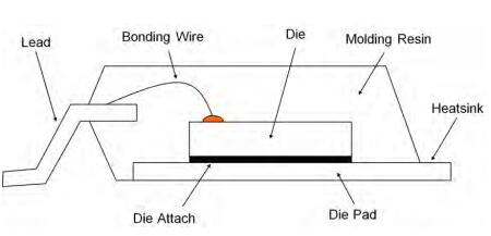
1. Packaging Structure
2. Package Specifications
|
Package Name
|
TO252-3
|
|
Type
|
TO
|
|
Pin Count
|
3
|
|
Package Weight [g]
|
0.29
|
|
Lead Finish
|
Pure Tin
|
|
MSL Level
|
1
|
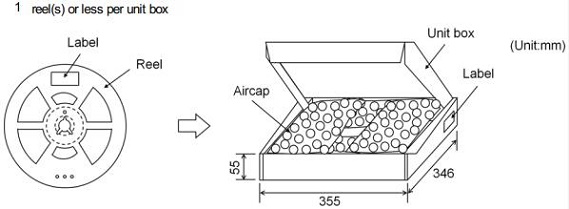
3. Packing Method
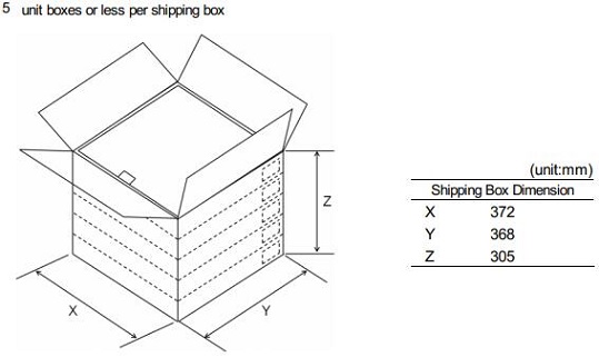
4. Packing Style
PSOP-8
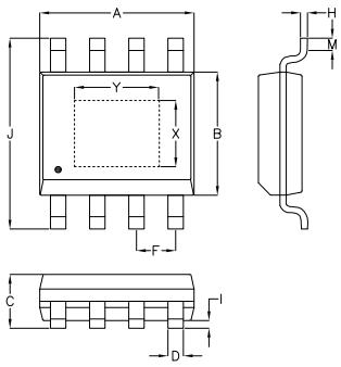
1. PSOP-8 Package Arrangement
2. PSOP-8 Package Pinouts
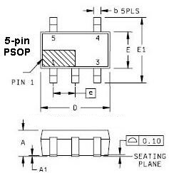
Figure 4: 5-pin PSOP IC Package
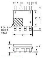
Figure 5: 8-pin PSOP IC Package
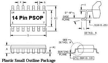
Figure 6: 14-pin PSOP IC Package
Plastic Small-Outline Package (PSOP) components have a high pin density, small pin spacing. As a general rule a surface mount SOP package is available that could replace any through hole DIP IC.
SOT-223
1. SOT223 Package Outline
|
Package information
|
Package name
|
Package description
|
|
SOT223
|
SC-73
|
Plastic, surface-mounted package with increased heatsink; 4 leads; 2.3 mm pitch; 6.5 mm x 3.5 mm x 1.65 mm body
|
2. Soldering
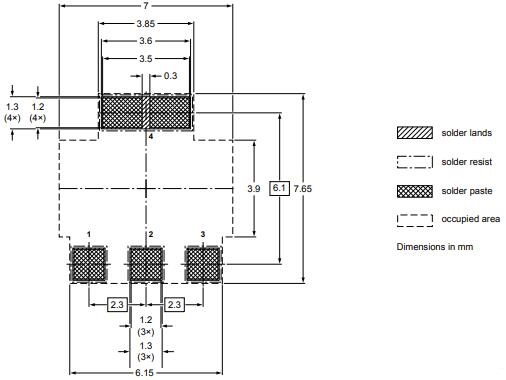
Figure 7: Reflow soldering footprint for SC-73 (SOT223)
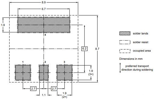
Figure 8: Wave soldering footprint for SC-73 (SOT223)
SOT-89-3
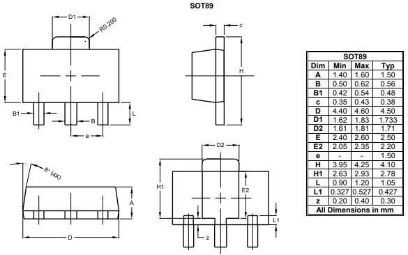
1. SOT89 Package Outline
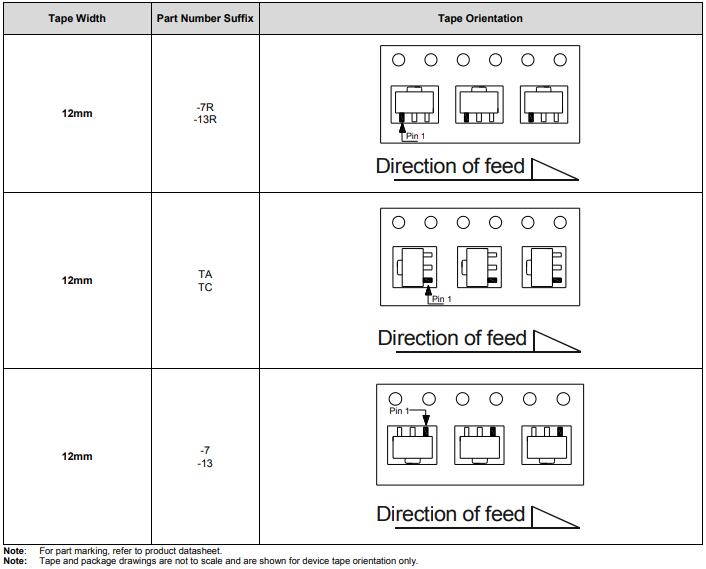
2. Device Tape Orientation
SOT-23-5
1. SOT-23-5 Package Outline
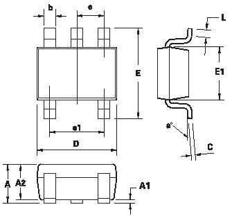
2. Package Information
1) Norminal weight
* Per device 12mg
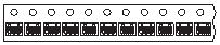
2) Tape and reel info
|
Orientation
|
Tape width (nm)
|
Reel size (inches)
|
No. Of components
|
Tape option indicator
|
|
|
8
|
7
|
3,000
|
TA
|
|
8
|
13
|
10,000
|
TC
|
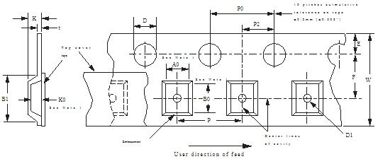
3. Embossed carrier tape configuration
LDO Pros and Cons
1. Advantages
(1) Simple structure, few peripheral components, and easy to use.
(2) There is no switching noise and can be used in analog circuits that require high precision and low noise.
2. Disadvantages
(1) It can only lower the voltage.
(2) Low efficiency, especially when the input voltage is high, and generally used when the load current is less than 1A.
Applications
1. In AC/DC Power Supply Circuit
Figure 14 is a schematic diagram of the application of low dropout regulator in AC/DC power supply.
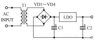
Figure 14: A LDO in AC/DC Power Supply Circuit
In this circuit, the alternating current is stepped down through the power transformer to obtain an AC low voltage, and then passes through the rectifier and filter circuit to obtain an unstable DC voltage. Then, a stable DC power supply is obtained through a LDO, and it also eliminates AC noise in the circuit and suppresses ripple voltage.
2. In Battery Power Circuit
Figure 15 is a schematic diagram of the application of a LDO in a battery power circuit.
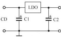
Figure 15: A LDO in Battery Power Circuit
The power supply voltage of the battery will change within a certain range. As the use time of the battery increases, its output voltage will decrease, after adding a low-voltage linear regulator to the circuit, the DC working state can be stable, even the battery or accumulator is nearly discharged, which increases the service life of the battery or accumulator.
3. In Switching Power Supply Circuit
Figure 16 is a schematic diagram of the application of a LDO in a switching power supply circuit.
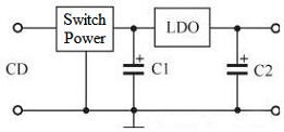
Figure 16: A LDO in a Switching Power Supply Circuit
When the input DC voltage is much higher than the required, a switching power supply circuit can be added before the LDO circuit, because it has unique advantages, such as high efficiency, large difference between input voltage and output voltage, etc. However, it also has many shortcomings, especially when used in analog circuits, such as high output ripple voltage, large noise, poor voltage regulation rate, etc.
So the above method can integrate the advantages of the two circuits. LDO can realize active filtering, remove interference, and greatly improve the voltage stabilization accuracy. In addition, the power supply system has no significant drop in efficiency either.
4. In Multi-channel Mutually Isolated Power Supply Circuits
Figure 17 is a schematic diagram of the application of a LDO in a multi-channel isolated power supply circuit.
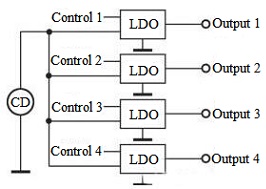
Figure 17: A LDO in a Multi-channel Isolated Power Supply Circuit
In some applications, such as communication equipment, one main power supply is often used, and multiple sets of small power supplies are required, which isolate from each other. That is, some of the small power supplies are working and others are not in order to save power. At this time, you can use multiple sets of LDO circuits, and control the on and off of the integrated circuits.
Classic Linear Regulator 1117 Series
1. Classic Circuits
AMS1117 is a relatively classic linear voltage regulator. In addition, TI’s TLV1117, ON Semi’s NCP1117, and Jiangsu Changjing Electronics Technology’s CJT1117 have also launched similarly Pin-to-Pin products. And SOT-223 is a typical package way of this series chips. The following schematic diagram illustrates the functions of its pins:
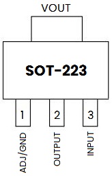
Figure 18: SOT-223 Package Top View
The following is a typical application circuit of the fixed voltage output version 1117. It is recommended to use a 10uF tantalum capacitor as the bypass capacitor C1, and another one as the output capacitor:
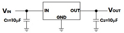
Figure 19: Typical Application Circuit – Fixed Output Versions
The figure below is a typical 1117 application circuit of the adjustable voltage output. Its output voltage formula is:

Where, IADJ (about 50uA) in the formula can usually be ignored because its value is much smaller than the current on R1 (about 2mA ~ 10mA).
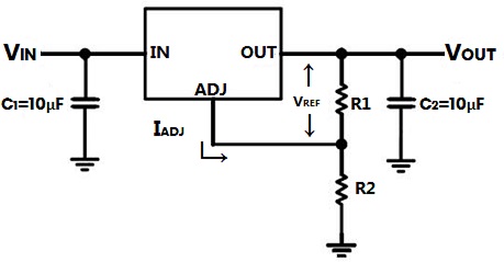
Figure 20: Typical Application Circuit–Adjustable Output Version
2. Output Voltage Accuracy
The output voltage accuracy of the 1117 series linear regulator is usually about ±1.5% of the nominal voltage value. That is, if the nominal output voltage is 3.3V, the actual output voltage should be between 3.25V ~ 3.35V:
|
Parts
|
Output Voltage (No-load)
|
Output Voltage (Full-load)
|
|
AMS1117
|
3.33V
|
3.3V
|
|
TLV1117
|
3.27V
|
3.26V
|
|
NCP1117
|
3.31V
|
3.3V
|
|
ME1117
|
3.28V
|
3.26V
|
|
CJT1117
|
3.32V
|
3.32V
|
Note: No-load output refers to the output voltage value when the output current is 0mA, while full-load output refers to the output voltage value of the 1117 chip when the output current is 800mA.
3. Output Ripple Control
Output ripple is a measure of the smoothness of a linear regulator's output voltage. It is an AC component superimposed on the DC stable value. Usually, this ripple only needs to be controlled within 20mV to meet normal use.
|
Parts
|
Output Voltage Ripple (No-load)
|
Output Voltage Ripple (Full-load)
|
|
AMS1117
|
17.6mV
|
19.2mV
|
|
TLV1117
|
16.2mV
|
18.4mV
|
|
NCP1117
|
15.8mV
|
16.8mV
|
|
ME1117
|
16.7mV
|
17.6mV
|
|
CJT1117
|
16.2mV
|
16.8mV
|
4. Dynamic Voltage Fluctuations
Because the downstream load of a linear voltage regulator usually changes dynamically, it will cause its output voltage to fluctuate. This fluctuation is a very important parameter to measure the performance of a linear voltage regulator.
|
Parts
|
Fluctuation Voltage
|
|
AMS1117
|
344mV
|
|
TLV1117
|
94mV
|
|
NCP1117
|
134mV
|
|
ME1117
|
216mV
|
|
CJT1117
|
172mV
|
Note: Usually the output capacitor of the 1117 series requires the use of tantalum capacitors instead of ceramic capacitors. This is because the parasitic resistance of tantalum capacitors is larger, while the parasitic resistance of ceramic capacitors is smaller. In other words, the power loop stability of the 1117 series relies heavily on tantalum capacitors with larger parasitic resistance, thereby improving its dynamic response performance.
5. Selection
Normally, the maximum output current of the 1117 series is 1A, but when converting from 5V to 3.3V and the output current is 800mA, the heating temperature of the chip will reach about 130°C, so try not to let the 1117 load higher than 1W.
Since the SOT-223 package size is large, it wastes PCB wiring space, and ceramic capacitors cannot be used as filter capacitors, and meanwhile, the quiescent current is relatively large (mAmp level), so it is not suitable for low-power consumption scenarios.

 English