Analog circuits refer to circuits used to transmit, transform, process, amplify, measure and display analog signals (continuously changing electrical signals). They are the basis of electronic circuits, including amplifier circuits, signal calculation and processing circuits, oscillation circuits, modulation and demodulation circuits, and power supplies. Let’s take 20 typical analog circuits as examples to analysis.
Analog Circuit Examples List
1. Bridge Rectifier Circuit
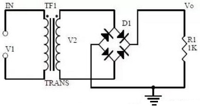
Key points:
1. Unidirectional conductivity of diode:
When a forward voltage is applied to the PN junction of the diode, it is in a conducting state; when a reverse voltage is applied, it is in a cut-off state.
Figure 2: Volt-ampere Characteristics Curve
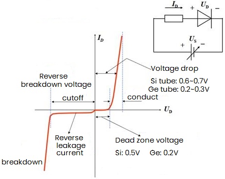
2. Ideal switching model and constant voltage-drop model:
It means that when the diode is forward biased, its tube voltage drop is 0V, and when reverse biased, its resistance is considered to be infinite and the current is zero. And the constant voltage drop model means that when the diode is turned on, its voltage drop is a constant value, 0.7V for silicon tubes and 0.5V for germanium tubes.
When u2 is the positive half cycle, the diodes Vd1 and Vd2 are turned on; while the diodes Vd3 and Vd4 are turned off, the current of the load RL flows through the load from top to bottom, and the same voltage as the positive half cycle of u2 is obtained on the load. In the negative half cycle of u2, the actual polarity of it is positive down and negative up, where the diodes Vd3 and Vd4 are turned on and Vd1 and Vd2 are turned off, and the current on the load RL still flows through the load from top to bottom, finally the load gets the same voltage for u2 positive half cycles.
3. Calculation:
Vo, Io, diode reverse voltage
Uo=0.9U2, Io=0.9U 2/RL, URM=√2U2
2. Power Filter
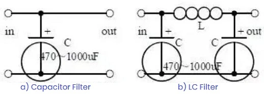
Key points:
1. Filtering Process Analysis:
Power filter is to connect a larger-capacity capacitor in parallel at both ends of the load RL. Since the voltage across the capacitor cannot change suddenly, the voltage across the load will not change suddenly either, so that the output voltage can be smoothed to achieve the purpose of filtering.
Waveform formation process:
Connected the output terminal to the load RL, when the power supply is powered, it provides current to the load and also charges the capacitor C. The charging time constant is τcharge = (Ri∥RLC)≈RiCl, Ri in general, and the influence of the voltage drop of Ri is ignored, and the voltage on the capacitor will rise rapidly with u2. When ωt=ωt1, u2=u0; then u2<u0, all diodes are cut off, the capacitor C discharges through RL, while the discharge time constant is RLC, the discharge is slowly, and u0 changes gently; when ωt=ωt2, u2= After u0, ωt2, u2 changes to be larger than u0 again, and the charge process starts again, and u0 rises rapidly. When ωt=ωt3, u2=u0, after ωt3, the capacitor is discharged through RL. The above process has been repeated. Due to the energy storage effect of capacitor C, the voltage fluctuation on RL is greatly reduced. Capacitor filter is suitable for situations where the current changes little, while LC filter circuit is suitable for situations where the current is large and the voltage ripple is small.
2. Calculation:
1) Selection of filter capacitor capacity and withstand voltage value
2) The output voltage Uo of the capacitor filter rectifier circuit is between √2U2~0.9U2, and the average value of the output voltage depends on the discharge time constant.
3) Capacitance RLC≧(3~5)T/2, where T is the cycle of AC power supply voltage. In practice, it is often further approximated as Uo≈1.2U2. The maximum reverse peak voltage of the rectifier is URM=√2U2, and the average current of each diode is half the load current.
3. Signal Filter
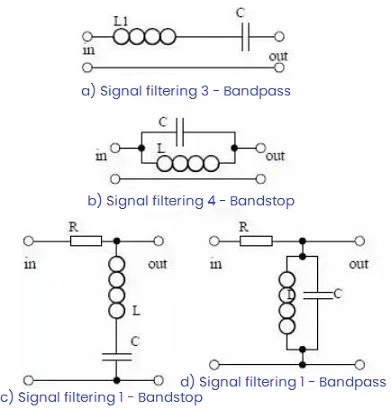
Key points:
1. The function of signal filter:
Attenuate the unwanted signal components in the input signal to a small enough level, but at the same time, the useful signal must be allowed to pass smoothly.
Compared with power filter:
The difference between the two is: the signal filter is used to filter the signal, and its passband is a certain frequency range, while the power filter is used to filter out the AC component and allow DC to pass through, thereby keeping the output voltage stable, and the AC power supply only allows a specific frequency passes.
The similarity: they all work with the amplitude-frequency characteristics of the circuit.
2. Impedance calculation of LC series and parallel circuits:
1) When in series connection, the circuit impedance is Z=R+j(XL-XC)=R+j(ωL-1/ωC).
When in parallel connection, the impedance of the circuit is
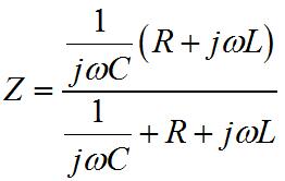
In practice, R<ωL is in general, so
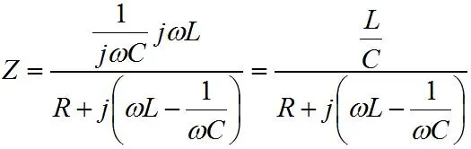
2) Amplitude-frequency curve and phase-frequency curve:
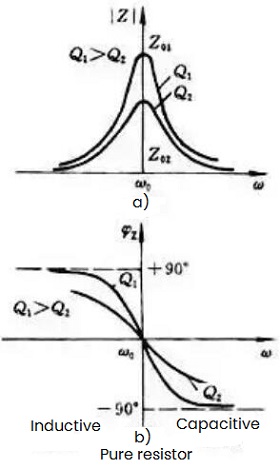
3. Draw the passband curve:
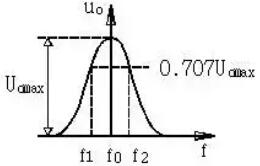
Calculate the resonant frequency: fo=1/2π√LC
4. Differential Circuit and Integral Circuit
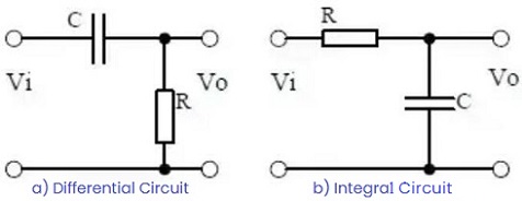
Key points:
1. The function of the circuit, the differences and similarities with the filter.
2. Analyze the voltage change process of differential and integral circuits and draw voltage change waveform diagrams.
3. Calculation: time constant, voltage change equation, selection of resistance and capacitance parameters.
5. Common Emitter Amplifier Circuit
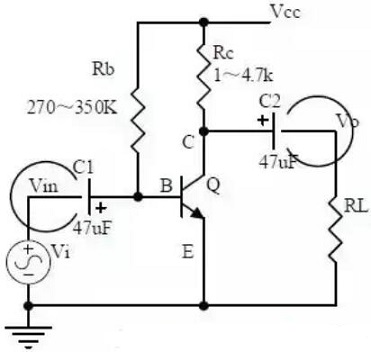
Key points:
1. The structure of the transistor, the current relationship between each pole, the characteristic curve, and the amplification conditions.
2. The functions of components, the purpose of circuits, voltage amplification factors, input and output signal voltage phase relationships, AC and DC equivalent circuit diagrams.
3. Calculation: static operating point and voltage amplification factor.
6. Common Emitter Amplifier Circuit (Voltage Divider Bias)
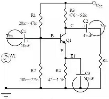
Key points:
1. The functions of components, the purpose of circuits, voltage amplification factors, input and output signal voltage phase relationships, AC and DC equivalent circuit diagrams;
2. Analysis of the current series negative feedback process and the impact of negative feedback on circuit parameters.
3. Calculation: static operating point and voltage amplification factor
4. Have controlled source equivalent circuit analysis
7. Common Collector Amplifier Circuit (Emitter Follower)
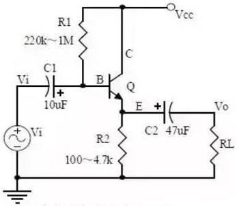
Key points:
1. The role of components, the purpose of the circuit, voltage amplification factor, signal voltage phase relationship between input and output, AC and DC equivalent circuit diagrams, and input and output impedance characteristics of the circuit.
2. Analysis of the current series negative feedback process and the impact of negative feedback on circuit parameters.
3. Calculation: static operating point and voltage amplification factor
8. Circuit Feedback Block Diagram
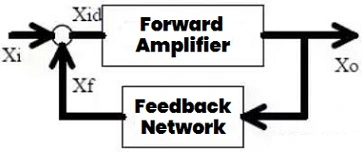
Key points:
1. The concept of feedback, positive and negative feedback and their judgment methods, parallel feedback and series feedback and their judgment methods, current feedback and voltage feedback and their judgment methods.
2. Amplification gain with negative feedback circuit
3. The impact of negative feedback on the amplification gain, passband, gain stability, distortion, input and output resistance of the circuit.
9. Zener Diode Circuit (Simple)
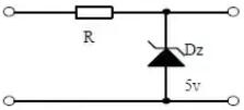
Key points:
1. Characteristic curve of Zener diode
2. Things to note when applying Zener diodes
3. Analysis of voltage stabilization process
10. Series Regulated Power Supply
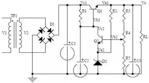
Key points:
1. Block diagram of series regulated power supply
2. The functions of each component, and analysis of the voltage stabilization process
3. Calculation: output voltage
11. Differential Amplifier Circuit
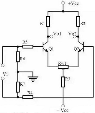
Key points:
1. The function of each component of the circuit, the purpose of the circuit, and the characteristics of the circuit.
2. Analysis of the working principle of the circuit, and How to amplify differential mode signals and suppress common mode signals.
3. Single-ended input and double-ended input, single-ended output and double-ended output working modes of the circuit.
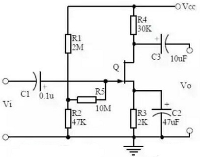
12. FET Amplifier Circuit
Key points:
1. The classification, characteristics, structure, transfer characteristics and output characteristic curve of field effect transistors.
2. Characteristics of FET amplifier circuit
3. Applications of FET amplifier circuit
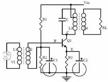
13. Frequency Selective Amplifier (Passband)
Key points:
1. The function of each component, the characteristics of the frequency selective amplifier circuit, and the function of the circuit.
2. Calculation of characteristic frequencies and selection of frequency-selective component parameters.
3. Amplitude-frequency characteristic curve
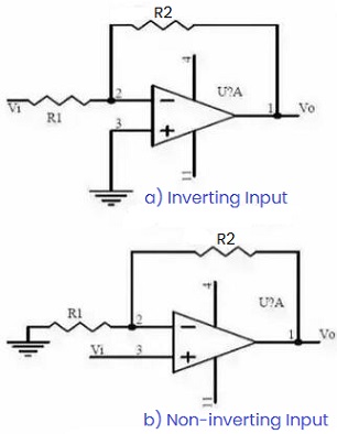
14. Operational Amplifier Circuit
Key points:
1. The concept of an ideal operational amplifier, the input terminal of the operational amplifier is a virtual short circuit, and the input terminal of the operational amplifier is a virtual open circuit.
2. The main purpose of the inverting op amp circuit is the phase relationship between the input voltage and the output voltage signal.
3. Gain expression, input impedance, and output impedance in non-inverting input mode.
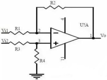
15. Differential Op Amp Circuit
Key points:
1. Characteristics and uses of differential operational amplifier circuits
2. The relationship between the output signal voltage and the input signal voltage.
16. Voltage Comparator Circuit
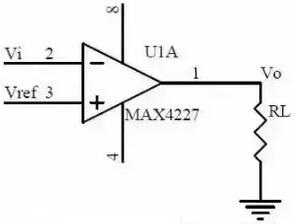
Key points:
1. The function and working process of the voltage comparator
2. Input-output characteristic curve of the comparator
3. How to construct a hysteresis comparator.
17. RC Oscillator Circuit
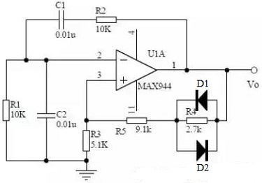
Key points:
1. The composition and function of the oscillation circuit, the phase conditions for oscillation, and the conditions for oscillation and balance amplitude.
2. The RC circuit impedance-frequency curve, and the phase-frequency curve.
3. Analysis of the phase conditions of the RC oscillation circuit, oscillation frequency, and components selection.
18. LC Oscillator Circuit
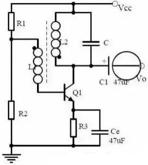
Key points:
1. Analysis of oscillation phase conditions.
2. DC equivalent circuit diagram and AC equivalent circuit diagram.
3. Calculation: oscillation frequency.
19. Quartz Crystal Oscillator Circuit (Series)
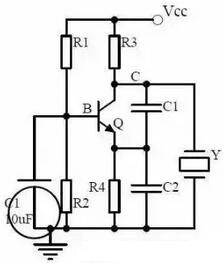
Key points:
1. Characteristics of quartz crystal, equivalent circuit of quartz crystal, characteristics of quartz crystal.
2. Characteristics of quartz crystal oscillators.
3. The oscillation frequency of the quartz crystal oscillator.
20. Power Amplifier Circuit
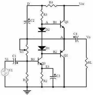
Key points:
1. The working process and crossover distortion of Class B power amplifier.
2. Composite rules for composite transistors.
3. Working principles and characteristics of Class A and Class B power amplifiers, and bootstrapping process.

 English










