The switched-mode power supply (SMPS) topology controls the output of the power through the switching tube, allowing it to operate at high frequency, thereby improving efficiency. Circuit topology is the connection method of power devices and electromagnetic components in the circuit, here are 14 common topology structures of switching-mode power supplies. And we will learn more about the half-bridge, full-bridge and push-pull topology structures.
Topology Structures of SMPS
Half Bridge
The primary side of the half-bridge transformer is composed of two capacitors and two high-voltage transistors connected diagonally. The two capacitors divide the input voltage into two, when the two transistors are disconnected, the voltage stress on the primary side of switch tube is reduced, so it is used by many high-voltage switching power supplies.
Switches S1 and S2 are alternately turned on, causing the primary side of the transformer to form an AC voltage with an amplitude of Ui/2, and the secondary side is equivalent to being connected to a buck circuit, so changing the switch duty cycle can change the output voltage Uo. The basic topology is shown in Figure 1:
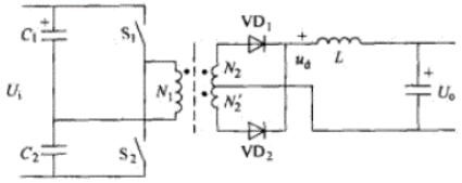
Figure 1: Basic Half Bridge Converter Topology
Working Principle
1. Continuous Current Mode
When the half-bridge circuit is in continuous operation mode, it experiences four switching states in one switching cycle, among which state 2 and state 4 are the same. As shown below:
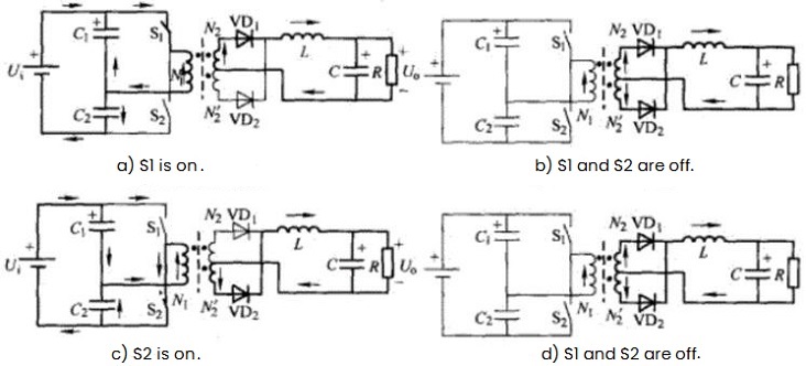
Figure 2: 4 Switched Modes (Half Bridge)
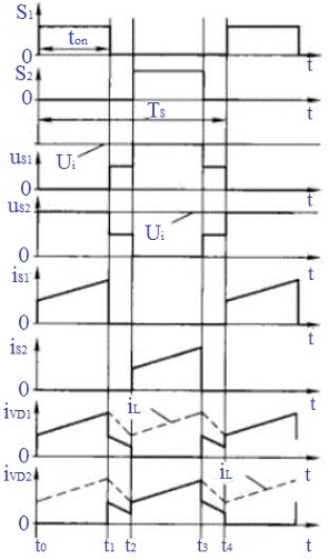
Figure 3: The Continuous Current Waveform
State 1: t0~t1, S1 is on and S2 is off.
At this time, the capacitor C1 charges the transformer, forming a current flowing from the same terminal on the primary side. According to Lenz's law, the secondary side of the transformer will generate a current flowing out from the same terminal to blocks the magnetic flux increase. While the diode VD1 of the upper winding is turned on, forming a loop: upper winding N2 → diode VD1 → inductor L → load R. And the inductor current rises linearly and then charged. The current output by the same terminal of the lower winding is cut off by the diode VD2 and cannot form a loop. This is equivalent to that under ideal circumstances, the energy of the capacitor C1 is transferred to the transformer. The transformer then transfers the energy from the primary side to the secondary side through magnetic coupling, then the secondary side then transfers the energy to the inductor through the induced electromotive force generated.
State 2: t1~t2, S1 and S2 are both disconnected.
At this time, the primary coil current of the transformer is 0, and the current in the inductor L cannot change suddenly. In order to maintain the magnetic potential balance of the transformer, the lower winding of the transformer will share half of the inductor current, and the direction is opposite to the direction of the upper winding current. Finally, the diodes VD1 and VD2 conduct, and the inductor L discharges.
State 3: t2~t3, S1 is disconnected and S2 is on.
This state is similar to state 1, except that the energy transfer starts from C2. The current loop formed by the secondary side is: lower winding N2'→diode VD2→inductor L→load R, the inductor current rises linearly and the inductor is charged.
State 4: t3~t4, S1 and S2 are both disconnected, this state is the same as state 2.
When inverting DC into AC through switches, it is necessary to avoid short circuit caused by S1 and S2 being turned on at the same time. And the conduction time of each switch cannot exceed 50%*TS, and a margin must be left, as shown by ton in the waveform diagram.
The input-output relationship can be derived based on the volt-second product balance of the inductor:

Where,

2. Discontinuous Current Mode
At this time, the circuit goes through six states in one cycle, as shown in Figure 4:
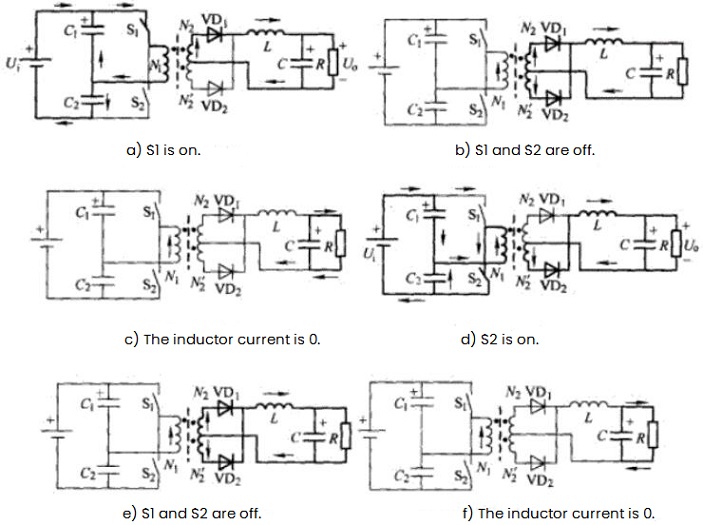
Figure 4: 6 Switched Modes
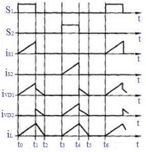
Figure 5: The Discontinuous Current Waveforms
State 1: t0~t1, consistent with continuous current mode state 1.
State 2: t1~t2, consistent with continuous current mode state 2.
State 3: t2~t3, the inductor current remains at 0, and the output is maintained by relying on the capacitor, which is the same as the buck circuit discontinuous mode.
State 4: t3~t4, consistent with continuous current mode state 3.
State 5: t4~t5, consistent with continuous current mode state 4.
State 6: t5~t6, the inductor current remains at 0, and the output is maintained by relying on the capacitor, which is the same as the buck circuit discontinuous mode.
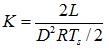
The input-output relationship is as following:
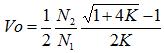
Where,
Full Bridge
The inverter circuit of the full-bridge converter consists of four switches. The two diagonal switches are turned on at the same time, while the switches on the same side are turned on alternately, inverting the DC power into AC power with an amplitude Ui, which is added to the primary side of transformer. Under this, the duty cycle of the switch changes, so does the output voltage. The basic topology is shown in Figure 6:
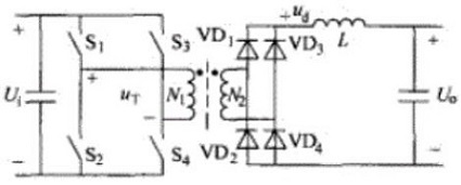
Figure 6: Basic Full Bridge Converter Topology
Working Principle
Only the current continuous mode is described here, and the analysis of the discontinuous mode is similar to the previous one. There are 4 states, as shown in Figure 7.
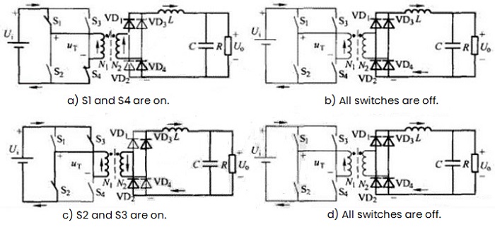
Figure 7: 4 Switched Modes (Continuous Current)
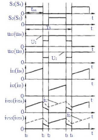
Figure 8: The Continuous Current Waveforms
State 1: t0~t1, S1 and S4 are on, and S2 and S3 are off.
At this time, the power supply charges the transformer, forming a current flowing from the same terminal on the primary side of the transformer. According to Lenz's law, the secondary side will generate current, which flows out of the terminal to prevent the increase in magnetic flux. While the diodes VD1 and VD4 on the secondary side are turned on, forming a loop: secondary side of the transformer → diode VD1 → inductor L → load R → diode VD4. The inductor current rises linearly.
State 2: t1~t2, S1, S2, S3, and S4 are all disconnected.
At this time, the diodes VD1, VD2, VD3, and VD4 are all conductive. Each diode flows through half of the inductor current, and the inductor L discharges.
State 3: t2~t3, S1 and S4 are disconnected, S2 and S3 are on.
This state is similar to state 1, the current loop formed by the secondary side is: transformer secondary side → diode VD3 → inductor L → load R → diode VD2, The inductor current rises linearly and the inductor is charged.
State 4: t3~t4, S1, S2, S3, and S4 are all disconnected. This state is the same as state 2.
When inverting DC into AC through switches, short circuit caused by the upper and lower switches being turned on at the same time should avoided. The conduction time of each switch cannot exceed 50%*TS, and a margin must be left, as shown by the ton in the waveform diagram. In addition, if the conduction time of S1, S4 and S2, S3 is asymmetric, there will be a DC component in the AC voltage Ur, which will cause magnetic saturation of the transformer. Here a capacitor can be connected in series on the primary side of the transformer to block the DC component.
The input-output relationship can be derived based on the volt-second product balance of the inductor:

Where,

Push Pull
The switches S1 and S2 of the push-pull transformer are turned on alternately, inverting the DC power into AC power with an amplitude Ui, and forming an AC voltage with opposite phases at both ends of the windings N1 and N1’. The transient voltage peak value S1 and S2 endure when the switch is turned off is 2Ui. Changing the duty cycle of the switch changes the output voltage. The basic topology is shown in Figure 9.
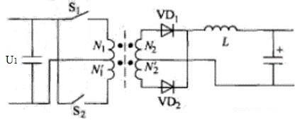
Figure 9: Basic Push Pull Converter Topology
Working Principle
Only the current continuous mode is described here, and the analysis of the discontinuous mode is similar to the previous one. There are 4 switching states, as shown in Figure 10.
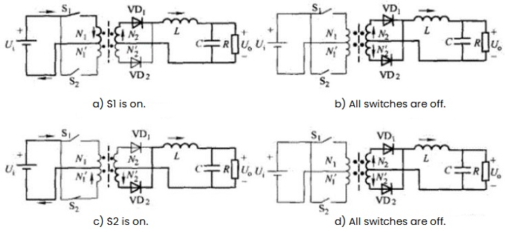
Figure 10: 4 Switched Modes of Push Pull Circuits (Continuous Current Mode).
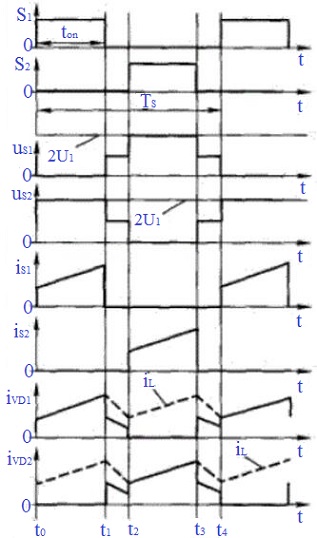
Figure 11: The Continuous Current Mode Waveforms
State 1: t0~t1, S1 is on, S2 is off.
The diode VD1 on the secondary side is on, and VD2 is off, forming a loop: secondary side of the transformer → diode VD1 → inductor L → load R, and the inductor current rises linearly.
State 2: t1~t2, S1 and S2 are both disconnected.
At this time, the diodes VD1 and VD2 conduct, each diode flows through half of the inductor current, and the inductor L discharges.
State 3: t2~t3, S1 is off, S2 is on.
This state is similar to state 1, the current loop formed by the secondary side is: transformer secondary side → diode VD2 → inductor L → load R, and the inductor current rises linearly.
State 4: t3~t4, S1 and S2 are both disconnected, this state is the same as state two.
When inverting DC into AC through switches, it should be avoided that the upper and lower switches are turned on at the same time, causing a short circuit in the transformer. The conduction time of each switch cannot exceed 50%*TS, and a margin must be left, as shown by the ton in the waveform diagram. In addition, if the conduction time of S1 and S2 is asymmetric, there will be a DC component in the AC voltage Ur, which will cause magnetic saturation of the transformer. Unlike the full-bridge circuit, the push-pull circuit cannot connect a capacitor in series with the primary side of the transformer, and the generation of DC component can only be avoided by accurately controlling the signal and matching circuit component parameters.
The input-output relationship can be derived based on the volt-second product balance of the inductor:

Where,


 English










