A flip-flop is a circuit that is used to automatically perform actions when specific conditions are met. It has two stable states that can be used to store binary data and can be changed by applying different inputs. Flip-flops are widely used in digital equipment, communication systems, industrial control equipment and other fields.
According to different logical functions, it can be divided into the following categories:
Flip-flop in Electronics
R-S Flip-flop
The R-S flip-flop is the most basic and simplest flip-flop, consisting of two cross-coupled inverting output Schmitt triggers. It can implement functions such as latching and synchronization, and is commonly used in digital logic circuits.
Usually composed of two NOR gates or NAND gates. Where S stands for Set and R stands for Reset. Then S_D is called the set end or the set 1 input end, and R_D is called the reset end or the set 0 input end. The basic RS flip-flop directs the output signal back to the input end, forming a feedback. This makes the state of the output signal related to the state of the input signal at the same time and the state before output.
NAND Gate Truth Table
|
A
|
B
|
Y
|
|
0
|
0
|
1
|
|
0
|
1
|
1
|
|
1
|
0
|
1
|
|
1
|
1
|
0
|
Basic Characteristics Table
|
R
|
S
|
Qn+1
|
|
1
|
0
|
1
|
|
0
|
1
|
0
|
|
1
|
1
|
Qn
|
|
0
|
0
|
Unstable
|
Putting the above two together is:
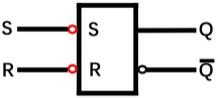
Figure 1: R-S Flip-flop in Digital Logic
The red circle indicates that R and S are both active low-level inputs.
Characteristic table meaning:
First row: R is the reset terminal, which is active at low level, that is, it is valid when R is 0; when S is 1 (the setting terminal is invalid), the output Q^(N+1) is 0.
Second row: S is the setting terminal, which is active at low level, that is, it is valid when S is 0, and when R is 1 (the reset terminal is invalid), the output Q^(N+1) is 1.
Third row: Inputs R and S are both 1, that is, when both the reset terminal and the setting terminal are valid, the output remains Q^N.
Prove:
Assume QN=1, then QN is not equal to 0:
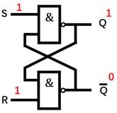
The first NAND gate inputs 1 and 0. According to the truth table of the NAND gate, the output of Q^(N+ 1) is 1.
The second NAND gate inputs 1 and 1. According to the NAND gate truth table, Q^(N+1) non-output is 0.
Q(N+1)=QN, the output remains unchanged.
Suppose QN=0, then QN is not equal to 1:
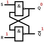
The first NAND gate inputs 1 and 1. According to the NAND gate truth table, the output of Q^(N+ 1) is 0.
The second NAND gate inputs 0 and 1. According to the truth table of the NAND gate, the non-output of Q^(N+1) is 1.
Q(N+1)=QN, the output remains unchanged.
Comprehensive two assumptions: when the inputs R and S are both 1, the output remains unchanged.
Fourth row:
When both R and S are 0, it is an unstable state. Try to avoid this state when using flip-flops.
When both R and S are input as 0:
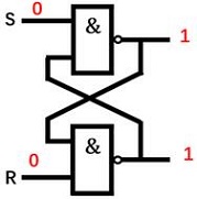
According to the characteristics of the NAND gate, the two output terminals are 1.
Sequence diagram analysis:
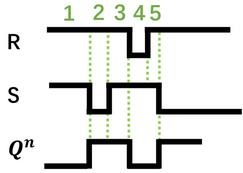
Figure 2: Timing Diagram
Status 1: The inputs of R and S are both 1, and the output remains unchanged and is still 0.
Status 2: R input is 1, S input is 0, and the output is set to 1.
Status 3: The inputs of R and S are both 1, and the output remains unchanged and is still 1.
Status 4: R input is 0, S input is 1, and the output is set to 0.
Status 5: R input is 1, S input is 0, and the output is set to 1.
D (Data/Delay) Flip-flop
A D flip-flop is a latch with a data input that changes state and outputs only when a clock pulse arrives. Its output value is equal to its data input value. D flip-flops are commonly used in circuits such as registers and flash memories.
The D flip-flop consists of six NAND gates. Its circuit diagram and logic symbols are shown in the figure below. Among them 5 and 6 constitute the basic RS flip-flop.
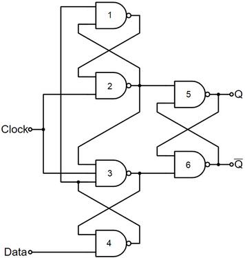
Figure 3: D Flip Flop Circuit Diagram
There are two triggering methods of D flip-flop: level trigger and edge trigger. The former can be triggered when CP (clock pulse) is 1, while the latter is mostly triggered on the leading edge of CP (positive transition 0→1).
The secondary state of the D flip-flop depends on the state of the D terminal before triggering. Therefore, it has two functions of setting 0 and setting 1. In addition, for edge D flip-flops, since the circuit has a maintaining blocking effect during CP=1, the data state change at the D terminal during CP=1 will not affect the output state of the flip-flop.
Logic symbol:
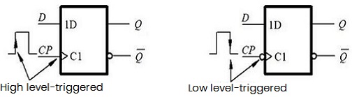
Figure 4: D Flip Flop in Digital Electronics
The state of the circuit before the arrival of the effective edge of CP is called the current state, represented by Q^n.
After the arrival of the effective edge of CP, the new state that the circuit enters is called the secondary state, represented by Q^{n+1}.
Characteristics table
|
D
|
Q^n
|
Q^{n+1}
|
|
0
|
0
|
0
|
|
0
|
1
|
0
|
|
1
|
0
|
1
|
|
1
|
1
|
1
|
After the trigger pulse, the output holds the excitation segment input signal, which can be used to create data registers.
Characteristic equation:

J-K Flip-flop
The J-K flip-flop is an asynchronous flip-flop similar to the SR flip-flop. The input includes clock, J, K and reset signals, and has two states: flip and hold. It can be used to design pipelines and pulse synchronization circuits, etc.
As for use, RS flip-flop does not allow R and S to be 1 at the same time, while the JK flip-flop allows J and K to be 1 at the same time. If not, the value state of the output will be toggled.
Timing Diagram
|
J
|
K
|
Action
|
Q
|
Qnext
|
Action
|
|
0
|
0
|
Hold state
|
x
|
x
|
No Change
|
|
0
|
1
|
Reset
|
x
|
0
|
Reset
|
|
1
|
0
|
Set
|
x
|
1
|
Set
|
|
1
|
1
|
Toggle
|
1(0)
|
0(1)
|
Toggle
|
Working Principle
A master-slave flip-flop can be edge triggered or level triggered, which means it can change its output state when transitioning from one state to another, i.e. edge triggered. While the output of a flip-flop changes when the input is high or low, that is, level triggered. In addition, in edge triggering, it can be +ve edge triggering or -ve edge triggering.
In edge triggering, the main trigger originates from the +ve edge of the clock pulse. At this time, the slave flip-flop is in a holding state, that is, the output of the master flip-flop is consistent with its input. When a negative clock pulse arrives, the slave flip-flop is activated, then the O/P of the master flip-flop is propagated through the slave flip-flop, and the master flip-flop is in the hold state.
The JK flip-flop master-slave overcomes the limitations of the SR flip-flop. In the SR flip-flop, when the S=R=1 condition is reached, the output becomes uncertain, while in the JK master slave, when J=K=1, the output flips, and this state of the output changes continuously with the clock pulse.
T (Toggle/Trigger) Flip–flop
A T flip-flop is a latch that completes state transitions under a clock signal. Its input is a T (switching) signal and the current output is inverted when the clock signal changes. It has only one signal input terminal T. When the valid edge of the clock arrives, the T terminal inputs a valid signal, and the flip-flop flips, otherwise the flip-flop remains unchanged. It is often used in frequency division circuits, counters and other applications.
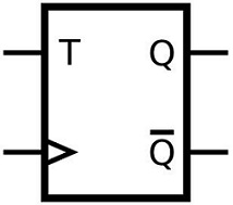
Figure 5: T flip-flop in Digital Logic
Characteristic equation:

Characteristic table:
|
T
|
Q
|
|
|
0
|
0
|
0
|
|
0
|
1
|
1
|
|
1
|
0
|
1
|
|
1
|
1
|
0
|
Flip-flop Triggered Modes
1. Level-triggered Mode
When the trigger signal is at a valid level, the input signal enters the flip-flop circuit and sets the flip-flop to the corresponding state. If it is invalid, the input signal is blocked and the trigger state is maintained.
1) Only when CLK becomes a valid level, the flip-flop can accept the input signal and set the flip-flop to the corresponding state according to the input signal.
2) During the entire time when CLK=1, changes in S and R will cause changes in the state of the flip-flop output.
3) If the input signal changes multiple times during CLK=1, the state of the flip-flop will also flip multiple times.
2. Edge-triggered Mode
It refers to receiving input data when a certain agreed transition (positive transition or negative transition) of the clock pulse CLK arrives. A flip-flop that does not receive data during CLK=l and CLK=0 and when a non-conventional transition of CLK arrives.
The secondary state of a flip-flop depends only on the logic state of the input when the rising edge (also known as the positive edge) or falling edge (also known as the negative edge) of the clock signal arrives. In addition, changes in the input signal have no effect on the output state of the flip-flop, which effectively improves the anti-interference ability of the flip-flop, thereby also improving working reliability.
3. Pulse-triggered Mode
Commonly used master-slave structure is implemented, that is, the master and slave flip-flops are connected in series, and the trigger signal is inverted. Taking the positive pulse trigger as an example, when the trigger signal is high, the input signal enters the main trigger and sets the main trigger state; after the trigger becomes low, the input signal is blocked and the main trigger state is maintained. At the same time, the slave trigger status is determined based on the main trigger status.
Action characteristics:
1) The flipping of the trigger occurs in two steps:
In the first step, during CLK=1, the master flip-flop receives the input signal, while the slave flip-flop does not move.
In the second step, when the falling edge of CLK arrives, the slave flip-flop flips according to the state of the master flip-flop, so the changes in the Q and Q' states occur on the falling edge of CLK (if CLK is a low-level valid signal, the Q and Q' states changes occur on the rising edge of CLK).
2) Because the main flip-flop itself is a level-triggered SR flip-flop, the input signal will control the main flip-flop during all the time CLK=1.

 English










