IP5306 PMIC
What Is IP5306?
IP5306 is a multi-function power management SoC that integrates a boost converter, lithium battery charging management, and battery power indicator, providing a complete power solution for mobile power supplies. The high integration and rich functions of IP5306 require only a few peripheral components for application, effectively reducing the size of the overall solution and reducing the BOM cost. IP5306 IC only needs one inductor to implement buck and boost functions, and can support low-cost inductors and capacitors. And its synchronous boost system provides a maximum output current of 2.4A and a conversion efficiency as high as 92%. When no-load, it automatically enters sleep state and the quiescent current drops to 100uA. The built-in IC temperature and input voltage intelligently adjust the charging current, and support 4 LEDs power display.
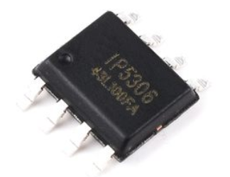
IP5306 Specifications
(1) Synchronous switch charging and discharging
· 2.4A synchronous boost conversion, 2.1A synchronous switch charging
· Boost efficiency up to 92%
· Charging efficiency as high as 91%
· Built-in power path management, supports charging and discharging simultaneously
(2) Charging
· Adaptive charging current adjustment, adaptive adapter
· Support 4.20/4.30/4.35/4.40V battery
(3) Battery display
· Support 4 LEDs power display
(4) Multi functions
· Button power on
· Built-in lighting driver
· Automatically detect phone insertion and removal
(5) Low power consumption
· Intelligent identification of load and automatic standby
· Standby power consumption is less than 100µA
(6) BOM minimalist
· Built-in power MOS, single inductor realizes charging and discharging
(7) Multiple protection and high reliability
· Output over-current, over-voltage and short-circuit protection
· Input overvoltage, overcharge, overdischarge, overcurrent discharge protection
· Over-temperature protection
· ESD 4KV, instantaneous withstand voltage 12V
(8) Deep customization
· Customized I2C interface with low-cost solutions
· Customized model IP5306_I2C
IP5306 Pins and Functions
Pin Configuration
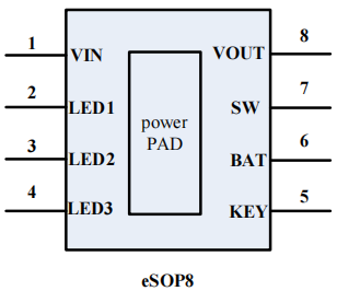
Figure 2: IP5306 Pin Configuration
Pin Function
|
NO.
|
Name
|
Function
|
|
Pin 1
|
VIN
|
DC5V charging input pin
|
|
Pin 2
|
LED1
|
LED driver pin
|
|
Pin 3
|
LED2
|
LED driver pin
|
|
Pin 4
|
LED3
|
LED driver pin
|
|
Pin 5
|
KEY
|
Key input, lighting driver multiplexing
|
|
Pin 6
|
BAT
|
Boost input pin, connected to the positive plate of the lithium battery
|
|
Pin 7
|
SW
|
DC-DC switch pin
|
|
Pin 8
|
VOUT
|
DC5V charging output pin
|
|
|
PowerPAD
|
GND
|
IP5306 in Use
IP5306 Typical Circuit
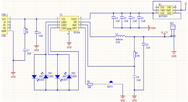
Figure 3: IP5306 Typical Circuit Application
In Figure 3, you can see that the circuit only uses a 1uH inductor, and no freewheeling diode of the traditional switching boost and buck circuit, because a MOS tube is integrated inside the device for synchronous rectification. This also improves the conversion efficiency of electrical energy.
IP5306 can drive up to 4 LED lights for power indicator and 1 lighting LED. For power indicator, it can be designed with less than or equal to 4 power indicator lights. In addition, this circuit also has a lighting LED lamp bead D5, which can be removed if it is not needed.
IP5306 can identify long key press and short key press operation, and the PIN5 pin is left floating when no key press is needed. The functions of the buttons in the circuit are as follows:
(1) The button duration is longer than 50ms but less than 2s, which is a short press action. A short press will turn on the battery indicator light and boost output.
(2) If the key duration is longer than 2s, it is a long press action. A long press will turn on or off the lighting LED.
(3) There will be no response for key presses less than 50ms.
(4) Two consecutive short presses within 1 second will turn off the boost output, power display and lighting LED.
If the IP5306 is not soldered well and you want to replace it, you need to pay special attention: the GND of the chip is the pad on the bottom. If the pad is not tinned before replacement, use a soldering iron to solder it directly. If not done properly, resulting in the GND on the chip not being connected to the GND on the PCB board, and the measured output voltage will very low, only 2-3V, and there is no boost. So it is necessary to care about the desoldering between the GND at the bottom of the chip and the PCB.
IP5306 Common Failures
1. Automatically sleep after half a minute of power on
It is mentioned in its datasheet that when the load automatic detection time TloadD load current continues to be less than 45mA for 32s, the chip will automatically enter the sleep state. However, in actual applications, the individual chips vary greatly. Some chips require a load current of more than 70mA to prevent automatic sleep, which is very unfriendly to products in the trial production stage.
* Solution:
1) When turning on the machine, input a 50ms pulse to the 5-pin KEY with a period of less than 30s.
2) Connect a resistor with a smaller resistance to the output end of the chip (the size is determined according to the actual required current), so that the current is large enough when the system works normally.
2. Keep shutting down and restarting
The chip keeps shutting down and restarting, which is probably caused by the chip detecting overcurrent or short circuit.
Overcurrent and short circuit detection explained:
1) The load overcurrent detection time TUVD output voltage continues to be lower than 4.4V for 50ms.
2) The load short circuit detection time TOCD output current continues to be greater than 4A for 150~200us.
* Solution:
A 100K and 100nF capacitor is added to the PMOS gate, which makes it take longer for the PMOS to turn on. And pay attention to the large capacitance at the output backend.
3. Chip burned out
Generally, chips will provide a variety of charge and discharge protection, but at the same time, we also need to pay attention to some situation. For example, you directly connected the battery without a protection board to the IP5306 battery pin according to the manual. Later, the chip often burned out after using the machine for a few weeks, and all the pins of the chip were connected to ground. When a low resistance state occurs, the battery continues to discharge and heat, causing the chip to burn out and the battery to be damaged.
* Multiple protection explained:
1) Output overcurrent, overvoltage and short circuit protection.
2) Input overvoltage, overcharge, overdischarge, overcurrent discharge protection.
3) The whole machine is over-temperature protected.
4) ESD 4KV, instantaneous withstand voltage 12V.
* Solution:
The battery is equipped with a protective board to prevent overshoot and overdischarge, which can effectively prevent the chip from burning.
The power management chip is an important integrated circuit used to manage and control power conversion in the power system to provide stable power supply. It has the characteristics of high integration, low power consumption, high efficiency and multi-function, and can play an important role in mobile devices, notebook computers, smart homes, industrial control and other fields. As the main control management IC, IP5306 is a functional power management power bank SOC that integrates a boost converter, lithium battery charging management, and battery power indication, providing a complete power solution for mobile power banks.

 English










