The MCP602 is a dual Operational Amplifier IC has a gain bandwidth product of 2.8MHz with low typical operating current of 230μA and an offset voltage that is less than 2mV. It uses Microchip's advanced CMOS technology, which provides low bias current, high-speed operation, high open-loop gain and rail-to-rail output swing. The MCP602 operates with a single supply voltage that can be as low as 2.7V, while drawing less than 325 of quiescent current per amplifier.
The device contains two independent op-amps in a single package, making it convenient for designs requiring multiple op-amps but wanting to save on board space and component count. Both the input and output voltage ranges can swing all the way from the negative supply voltage to the positive supply voltage, which is useful for single-supply applications, as well as for maximizing the output range.
MCP602 Alternative Parts
Here are some alternatives to the MCP602 that offer similar performance and may be suitable for similar applications:
Texas Instruments OPA1612 Series Audio Amplifiers
TI's OPA1612 (dual) bipolar-input operational amplifier achieves very low 1.1 nV/√Hz noise density with an ultra-low distortion of 0.000015% at 1 kHz. It offers rail-to-rail output swing to within 600 mV with a 2 kΩ load, which increases headroom and maximizes dynamic range. This device also has a high output drive capability of ±30 mA.
Also it operates over a very wide supply range of ±2.25 V to ±18 V, on only 3.6 mA of supply current per channel. The OPA1612 op amp is unity-gain stable and provides excellent dynamic behavior over a wide range of load conditions. The dual version features completely independent circuitry for lowest crosstalk and freedom from interactions between channels, even when overdriven or overloaded.
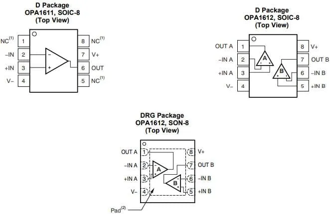
Figure 1: OPA1612 Pin Configuration and Functions
Key Features:
• Low distortion, low noise, and high-speed performance.
• High slew rate (27 V/µs).
• Rail-to-rail output with low total harmonic distortion.
• Automotive-grade options available.
• Professional audio equipment
• Microphone preamplifiers
• Analog and digital mixing consoles
• Broadcast studio equipment
• Audio test and measurement
• High-end A/V receivers
Applications:
• Professional Audio Equipment
• Microphone Preamplifiers
• Analog and Digital Mixing Consoles
• Broadcast Studio Equipment
• Audio Test And Measurement
• High-End A/V Receivers
Analog Devices ADA4927-1
The ADA4927 is a low noise, ultralow distortion, high speed, current feedback differential amplifier that is an ideal choice for driving high performance ADCs with resolutions up to 16 bits
from dc to 100 MHz. The output common-mode level can easily be matched to the required ADC input common-mode levels. The internal common-mode feedback loop provides exceptional output balance and suppression of even-order distortion products.
Differential gain configurations are easily realized using an external feedback network comprising four resistors. The current feedback architecture provides loop gain that is nearly independent of closed-loop gain, achieving wide bandwidth, low distortion, and low noise at higher gains and lower power consumption than comparable voltage feedback amplifiers.
The ADA4927 is fabricated using the ADI’s silicon-germanium complementary bipolar process, enabling very low levels of distortion with an input voltage noise of only 1.3 nV/√Hz. And the low dc offset and excellent dynamic performance of the ADA4927 make it well suited for a wide variety of data acquisition and signal processing applications.
The ADA4927-1 is available in a Pb-free, 3 mm × 3 mm 16-lead LFCSP. The pinouts are optimized to facilitate printed circuit board (PCB) layout and to minimize distortion. It is specified to operate over the −40°C to +105°C temperature range.
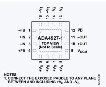
Figure 2: ADA4927-1 Pin Configuration and Functions
Key Features:
• Low noise and low distortion.
• High-speed performance with a slew rate of 60 V/µs.
• High-output drive and low total harmonic distortion.
• Automotive grade available.
• Applications:
• ADC drivers
• Single-ended-to-differential converters
• IF and baseband gain blocks
• Differential buffers
• Differential line drivers
STMicroelectronics TSZ182
The TSZ182 is a single and dual operational amplifier featuring very low offset voltages with virtually zero drift versus temperature changes.
The TSZ182 offers rail-to-rail input and output, excellent speed/power consumption ratio, and 3 MHz gain bandwidth product, while consuming just 1 mA at 5 V. The device also features an ultra-low input bias current.
The devices is suitable for high-accuracy high-bandwidth sensor interfaces.
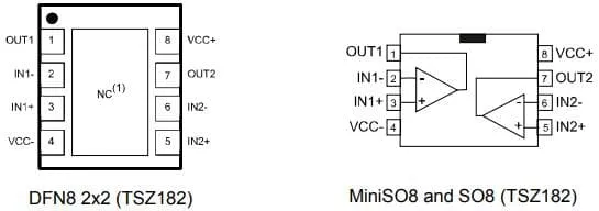
Figure 3: TSZ182 Pin Configuration and Functions
Key Features:
• High-speed performance with a wide bandwidth (100 MHz at -3 dB).
• High slew rate (50 V/µs).
• Rail-to-rail input and output
• Low supply voltage: 2.2 - 5.5 V
• Low power consumption: 1 mA max. at 5 V
• Precision voltage reference and low offset voltage.
Applications:
• Automotive and industrial electronics
• Signal conditioning
• Precision measurement
ON Semiconductor NCS2550
NCS2550 is a 750 MHz voltage feedback monolithic operational amplifier featuring high slew rate and low differential gain and phase error. The voltage feedback architecture allows for a superior bandwidth and low power consumption.
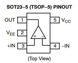
Figure 4: NCS2550 Pin Configuration and Functions
Key Features:
• High-speed, low-noise, and high-precision op-amp.
• High slew rate (30 V/µs) and wide bandwidth.
• Automotive-grade versions available.
Applications:
• Automotive sensor systems
• Line drivers
• Industrial controls
• Radar/communication receivers
Microchip MCP6V67
The Microchip Technology Inc. MCP6V67 operational amplifier provides input offset voltage correction for very low offset and offset drift.
The MCP6V67 has a gain bandwidth product of 1 MHz (typical). It is unity-gain stable, has virtually no 1/f noise and has good Power Supply Rejection Ratio (PSRR) and Common Mode Rejection Ratio (CMRR). It operates with a single supply voltage as low as 1.8V, while drawing 80 µA/amplifier (typical) of quiescent current.
The Microchip Technology Inc. MCP6V67 op amp is offered in dual MCP6V67 package. And it was designed using an advanced CMOS process.
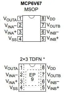
Figure 5: MCP6V67 Pin Configuration and Functions
Key Features:
• Low noise, low drift, and high speed.
• Available in both automotive and industrial-grade options.
• High slew rate (50 V/µs) and wide bandwidth.
Applications:
• Portable Instrumentation
• Sensor Conditioning
• Temperature Measurement
• DC Offset Correction
• Medical Instrumentation
Maxim Integrated MAX40000
The MAX40000 is a tiny, single comparator with built-in voltage references that are ideal for a wide variety of portable electronics applications, such as cell phones, portable instruments, and notebooks that have extremely tight board space and power constraints. It is available in a 6-bump waferlevel package (WLP) with 1.11mm x 0.76mm footprint and a 6-pin SOT23 package. The MAX40000 has a push-pull output and the MAX40001 has an open-drain output.
The device offers a supply voltage range from 1.7V to 5.5V and consume only 0.9μA of supply current. It also features internal filtering to provide high RF immunity, important in many portable applications.
The MAX40000 has a high-precision integrated reference that is factory trimmed to an initial accuracy of 1% and better than 2.5% over the entire temperature range. Internal reference voltage options include 1.252V, 1.66V, 1.94V, and 2.22V. Also you can buy a customized MAX40000 with a particular voltage reference value and package type, and the reference output is stable for capacitive loads up to 100pF.
The device is fully specified over -40°C to +125°C automotive temperature range. MAX40000 Pin Configuration and Functions
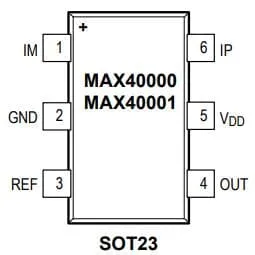
Figure 6: MAX40000 Pin Configuration and Functions
Key Features:
• Ultra-low offset voltage and high speed.
• Slew rate of 100 V/µs and wide bandwidth (180 MHz).
• Low input bias current.
• Input Voltage Range = -0.2V to 5.7V
• Supply Voltage Range (1.7V to 5.5V) allows operation from 1.8V, 2.5V, 3V, and 5V supplies
• <10μs Propagation Delay
Applications:
• Cell Phones
• Tablets and Consumer Accessories
• Notebook Computers
• Electronic Toys
• Portable Medical Instruments/Wearables
• Level Detectors
Analog Devices AD8021
The AD8021 is an exceptionally high performance, high speed voltage feedback amplifier that can be used in 16-bit resolution systems. It is designed to have both low voltage and low current noise (2.1 nV/√Hz typical and 2.1 pA/√Hz typical) while operating at the lowest quiescent supply current (7 mA @ ±5 V) among today's high speed, low noise op amps. The AD8021 operates over a wide range of supply voltages from ±2.25 V to ±12 V, as well as from single 5 V supplies, making it ideal for high speed, low power instruments. An output disable pin allows further reduction of the quiescent supply current to 1.3 mA.
The AD8021 is both technically superior and priced considerably less than comparable amps drawing much higher quiescent current. The AD8021 is a high speed, general-purpose amplifier, ideal for a wide variety of gain configurations, and can be used throughout a signal processing chain and in control loops. The AD8021 is available in both standard 8-lead SOIC and MSOP packages in the industrial temperature range of -40°C to +85°C.
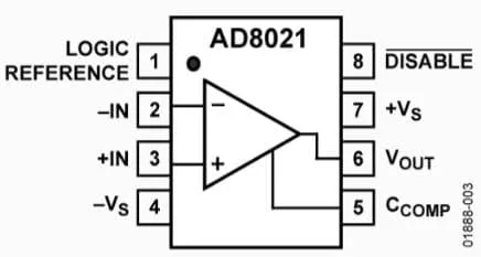
Figure 7: AD8021 Pin Configuration and Functions
Key Features:
• High-speed op-amp with low noise and low distortion.
• Slew rate of 12 V/µs and bandwidth of 8 MHz (typical).
• Automotive and industrial-grade options.
Applications:
• ADC preamps and drivers
• Instrumentation preamps
• Active filters
• Portable instrumentation
• Line receivers
• Precision instruments
• Ultrasound signal processing
• High gain circuits
Texas Instruments LMV358
The LMV358 device is single, dual, and quad low-voltage (2.7 V to 5.5 V) operational amplifiers with rail-to-rail output swing.
The device is the most cost-effective solutions for applications where low-voltage operation, space saving, and low cost are needed. It is designed specifically for low-voltage (2.7 V to 5V) operation, with performance specifications meeting or exceeding the LM358 and LM324 devices that operate from 5 V to 30 V. With package sizes down to one-half the size of the DBV (SOT-23) package, the LMV358 can be used for a variety of applications.
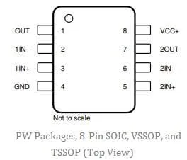
Figure 9: LMV358 Pin Configuration and Functions
Key Features:
• Dual operational amplifier with wide supply voltage range.
• Low power consumption and high-speed operation.
Applications:
• Desktop PCs
• HVAC: heating, ventilating, and air conditioning
• Motor control: AC induction
• Net-books
• Portable media players
• Power: telecom DC/DC module: digital
• Professional audio mixers
• Refrigerators
• Washing machines: high-end and low-end
Factors to Consider
LM61495QRPHRQ1 offers high power density, low EMI, and a wide range of configurable features to ensure optimal performance and reliability in various automotive environments. For more detailed information, you can refer to the datasheet provided by Texas Instruments. The following are some key factors you should consider:
• Package type: The LM61495QRPHRQ1 comes in the QFN-20 package, so make sure any replacement matches the required form factor (if applicable).
• Voltage range: Ensure the replacement op-amp supports the same voltage levels for your application.
• Temperature range: Automotive-grade op-amps often have a wider operating temperature range (-40°C to +125°C).
• Slew rate and bandwidth: Ensure the alternative op-amp meets or exceeds the required bandwidth and slew rate.
It should be noted that when replacing a specific component, please refer to the relevant datasheet.

 English










