With the rapid development of information technology, there is a growing demand for components in electronics to become increasingly lightweight and thin. For example, in personal computers, mobile phones, digital cameras, and video phones, it is necessary to regulate voltage to supply power to the circuits, and thin-film inductors are one of the key components in this process. The use of thin-film inductors allows three-dimensional magnetic core inductors to evolve into two-dimensional planar structures, significantly reducing the device size. Further more, the successful development of various high-frequency thin-film soft magnetic materials with low energy consumption, high initial permeability, high saturation magnetization, and a wide operating temperature range has made the production of high-frequency thin-film inductors a reality. So what is real thin-film inductor? Let’s have a look below.
What is Thin Film Tech?
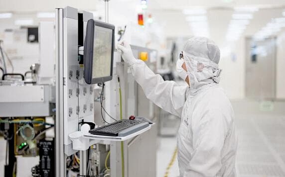
Thin film technology in semiconductors is a critical manufacturing process widely used in various fields such as electronics, solar energy, and optical devices. The following is a detailed explanation of the main knowledge points of thin film technology:
Manufacturing Process
The application of thin film technology in semiconductor manufacturing mainly includes the following key processes:
1. Chemical Vapor Deposition (CVD):
CVD is a method of depositing thin films on a substrate through gas-phase chemical reactions. It offers high precision, material diversity, and high purity, making it suitable for manufacturing various thin film layers in semiconductor devices.
The applications of CVD technology in semiconductor manufacturing include metal interconnects, gate dielectrics, and protective coatings.
2. Physical Vapor Deposition (PVD):
PVD includes methods such as sputtering and evaporation, which deposit materials onto a substrate through physical processes. PVD technology offers high adhesion strength and excellent surface finish in thin film deposition.
The applications of PVD technology in semiconductor manufacturing include the deposition of metal layers and dielectric layers.
3. Atomic Layer Deposition (ALD):
ALD is a method of depositing thin films layer by layer through self-limiting reactions, offering excellent step coverage and large-area uniformity. ALD technology is used in semiconductor manufacturing to precisely control film thickness and density.
The applications of ALD technology in semiconductor manufacturing include gate dielectrics, metal interconnects, and protective coatings.
Application Fields
Thin film technology is widely used in semiconductors, mainly including the following aspects:
1. Electronic devices:
Thin film technology is key to manufacturing electronic components such as transistors, sensors, and integrated circuits. For example, thin film transistors (TFTs) are widely used in flat panel displays and have the advantages of small size and low power consumption. Further more, the use of thin films in sensors can improve sensitivity and response time, which is suitable for applications such as environmental monitoring and medical diagnosis.
2. Solar cells:
Thin-film solar cells are made by depositing a layer of photovoltaic material on a substrate, which has the advantages of reducing the amount of materials used, reducing costs and weight. Thin-film solar cells can be flexibly adapted to different surfaces, expanding their application range.
3. Optical devices:
Thin film technology is used for optical coatings on lenses and glass to enhance properties such as transmission, refraction and reflection. For example, anti-reflective coatings on glasses and camera lenses can improve visibility, and UV filters can protect the eyes from harmful UV radiation.
4. Advanced applications:
Thin film technology is also used in more advanced applications such as quantum computers, smart windows and microfluidic systems. For example, smart windows use thin films to dynamically adjust transparency and control the light and heat entering the building.
Advantages
Translate the following text into English:
The application of thin film technology in semiconductors has many advantages:
1. Low power consumption:
Thin film technology uses thinner materials and consumes less power per unit area, which is suitable for energy-sensitive applications.
2. Cost-effectiveness and design flexibility:
Thin film manufacturing is generally cheaper and easier, and the design has greater flexibility, which is suitable for configurations such as single chip multi-chip (MCM) or multi-path interconnect (MPI).
3. High performance:
Thin film technology can achieve high-precision and high-purity thin film deposition, improving the performance and reliability of semiconductor devices.
Thin film technology plays a crucial role in semiconductor manufacturing, achieving high-precision and high-performance thin film deposition through various deposition processes such as CVD, PVD, and ALD. Its applications are extensive, including electronic devices, solar cells, optical equipment, and advanced technologies, offering advantages such as low power consumption, cost-effectiveness, and high performance. The continuous development of thin film technology will continue to drive innovation and progress in the semiconductor industry.
What is A Thin-film Inductor?
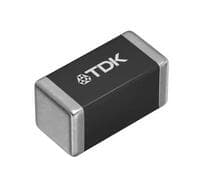
A thin film inductor is an inductor manufactured using vacuum thin film technology. It offers high reliability, ease of integration and miniaturization, making it highly suitable for automated surface mount technology (SMT). Due to its small size, high precision, and excellent high-frequency characteristics, it has become a research hotspot both domestically and internationally.
Manufacturing Process
Thin film inductors are manufactured using a process similar to that of integrated circuits (ICs). The main steps include:
1. Substrate Preparation: Coating a conductor film on the substrate.
2. Photolithography Process: Forming a coil pattern on the conductor film using photolithography technology.
3. Multilayer Structure: Adding dielectric layers, insulating layers, and electrode layers, and finally encapsulating the structure.
Design and Structure
1. Spiral Coil: Thin film inductors typically consist of spiral-shaped thin film coils that are placed on the substrate.
2. Material Selection: Common materials include aluminum oxide, microcrystalline glass, glazed, and polished alumina ceramic substrates.
3. High Precision: The coils are manufactured using microfabrication technology, resulting in high precision and stable inductance values.
Features and Advantages
1. Miniaturization: Due to their manufacturing process, thin film inductors can achieve very small sizes, making them suitable for compact electronic devices.
2. High Performance: They have a high Q value (quality factor), meaning low energy loss, which is suitable for high-frequency applications.
3. Stability: The inductance values are stable and less affected by temperature and vibration.
4. Low Noise: Due to their structure and material characteristics, thin film inductors typically have low noise levels.
Applications
The main uses of thin film inductors include filtering, energy storage, and oscillation circuits. Thin film inductors are manufactured using vacuum thin film technology and offer high reliability, ease of integration, and miniaturization, making them highly suitable for automated surface mount technology (SMT). Due to their small size and excellent high-frequency characteristics, thin film inductors perform exceptionally well in high-frequency applications, and with the well development of high-frequency thin-film soft magnetic materials, their use in high-frequency applications is becoming increasingly widespread.
• Application Scenarios:
1) Filtering: Thin film inductors can be combined with capacitors to form LC filters, effectively reducing noise levels in circuits and filtering out high-frequency noise and interference signals.
2) Energy Storage: Inductors can convert electrical energy into magnetic energy for storage, used in power supply filtering, oscillation circuits, and DC-DC conversion circuits.
3) Oscillation Circuits: Inductors play a crucial role in oscillation circuits, generating oscillation signals through the interaction between inductance and capacitance.
• Examples:
Thin film inductors are widely used in various electronic devices, mainly including:
1) Mobile Communication Devices: Such as mobile phones, wearable devices, etc.
2) Wireless and LAN Networks: Used for signal processing and transmission.
3) Power Supply: Used for filtering and voltage regulation.
4) Amplifiers and Oscillators: Used for signal amplification and frequency control.
Thin-film Inductor Newest Product
PLE856C Series Introduction
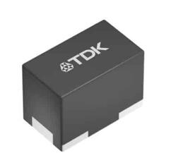
TDK recently announced the launch of the latest PLE856C series compact thin film power inductors for wearable devices. The new products will enter mass production starting this December.
As the functions and performance of wearable devices such as wireless earphones and smartwatches continue to enhance, the number of components installed within a single system is also increasing. However, the available space for such devices remains very limited, driving the demand for miniaturized electronic components. The inductance values of the PLE856C series range from 470nH to 1.5µH, making them the smallest inductors in the industry for internal power circuits of such devices, contributing to space-saving designs and lightweight devices. Compared to the traditional PLEA67B series, the newly launched PLE856C series reduces the required installation area by 40% and the volume by 50%, and its rated saturation current is between 0.40 A and 0.72 A.
Despite their compact size, the new products feature precisely formed coil conductor patterns as internal electrodes, thanks to TDK's proprietary thin film technology. Additionally, the new products use low-loss magnetic materials, which help reduce power loss while improving the efficiency of power circuits. In the future, TDK will fully leverage the advantages of thin film technology to continuously advance the development of smaller, high-performance inductors suitable for wearable devices and expand its lineup of power inductors to meet market demands.
Main Applications
• True wireless stereo earbuds
• Smartwatches
• AR/VR devices
• Small power modules
• Small communication modules
Key Features and Benefits
• The industry's smallest inductors for power circuits, helping to achieve space-saving device designs.
• Low-loss magnetic materials for efficient power circuits.
• High-precision internal electrodes formed using thin film technology.

 English










