Active Voltage Positioning (AVP) or active droop technology regulates power supply output: maintaining a higher output voltage under light load and a lower output voltage under heavy load. A significant benefit of implementing AVP control technology is improved load transient response and reduced output capacitance, as AVP provides greater scope for the power supply to respond to load transients. μModule regulators are complete, tested and qualified packaged power solutions. For telecommunications and data centre applications, μModule regulators are favoured for their rapid load transient response, minimal PCB footprint, and fully ceramic capacitor solutions. However, meeting all requirements proves challenging with conventional non-AVP control techniques.
This paper introduces a precise series AVP implementation method, incorporating two resistors within the feedback control loop. The advantage of this series AVP approach lies in its load line accuracy being virtually independent of changes in the gm amplifier gain. In contrast, other AVP implementations, such as shunt AVP1, exhibit reduced load line accuracy when significant variations occur in the gm amplifier gain. Implementing this series AVP reduces output capacitance by up to 50% while slightly improving peak-to-peak output voltage transients. The 50% capacitance reduction necessitates only ceramic capacitors, significantly enhancing system reliability and optimising costs. Aluminium electrolytic capacitors offer substantially lower reliability and higher costs compared to ceramic equivalents.
A further benefit of implementing AVP control technology lies in its ability to reduce output voltage during high load currents, thereby lowering load power dissipation. The LTM4650-2 example demonstrates a net power saving of 1.4 W or 5.6%, substantially reducing power consumption and extending battery runtime.
Serial AVP Implementation
AVP refers to a method whereby the output voltage of a voltage regulator dynamically adjusts in response to changes in load current. In contrast, traditional methods (non-AVP) maintain the output voltage fixed at the nominal value VOUT under all load conditions, as illustrated in Figure 1. When employing the AVP method, the output voltage progressively decreases as the output current increases. Under light load conditions, the output voltage is set to adjust to a level slightly above the nominal value. Under heavy load conditions, the output voltage is set to adjust to a level slightly below the nominal value. 1 When load current increases abruptly, the output voltage commences from a level above the nominal value. Consequently, it can decrease to a greater extent while remaining within the rated voltage range. When load current decreases abruptly, the output voltage commences from a level below the nominal value. Consequently, it can overshoot to a greater extent while remaining within the rated voltage range. For all load current ranges, the output voltage shall be constrained within the rated voltage limits (between VMAX and VMIN).
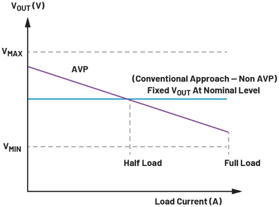
Figure 1. VOUT using AVP versus fixed nominal VOUT using conventional methods (non-AVP).
Figure 2 illustrates the AVP series compensation circuit. The internal reference voltage (VREF) and VOUT feedback are connected to the positive and negative inputs of the error amplifier respectively. VHI (or INTVCC), connected to RHI, supplies the appropriate DC voltage to the amplifier output (ITH or COMP) to prevent the output from entering saturation. RLO (the feedback resistor) is positioned between the output (ITH) and the negative input (or FB). Consequently, RLO determines the amplifier's gain (gm). The values of RHI and RLO should be substantially higher than those of R1 and R2.
Load line formula 1:

Ki denotes the current sensing gain, while RSENSE represents the current sensing resistor value (or the DCR value of the inductor when DCR sensing is employed).
Compared to the AVP shunt compensation circuit, the series compensation circuit offers the advantage that its load line depends on the R1/RLO gain, being virtually independent of the tolerance of the error amplifier's transconductance (gm). Integrated circuit processes and designs vary considerably. Regrettably, some ICs exhibit gm variations of up to ±30% between devices, and the load line of the shunt compensation circuit AVP is proportional to the gain 1/gm. Consequently, the load line of the shunt AVP is inferior.
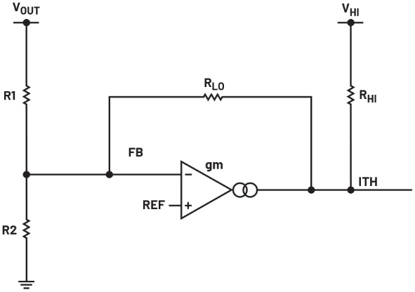
Figure 2. AVP Series Compensation Circuit
AVP Solution for the LTM4650-2 Voltage Regulator
On the LTM4650-2 (current-mode synchronous buck regulator), the nominal 1 V output can supply a 25 A load with a transient window of approximately ±8% (160 mV peak-to-peak). In such conventional regulators (non-AVP), an external RC filter circuit is required to achieve fast Type II control loop compensation. The output stage incorporates a bank of five 100 μF ceramic capacitors and two 470 μF POSCAP capacitors. When subjected to a 19 A load step (75% of full load) with a slew rate of 19 A/μs, the transient response exhibits a peak-to-peak voltage of 136 mV, as illustrated in Figure 3.
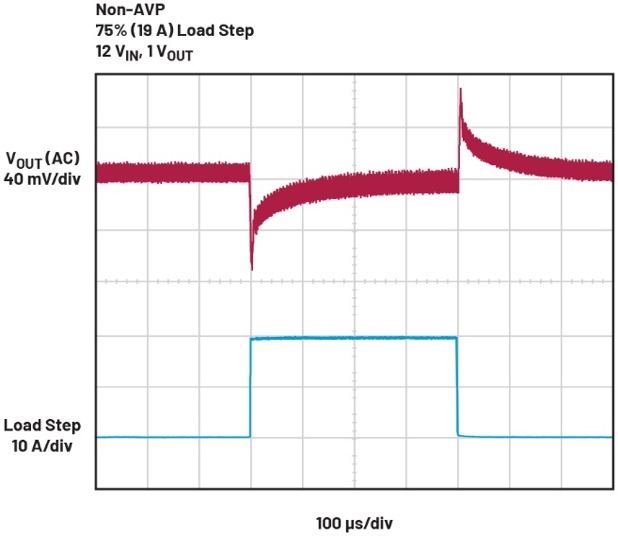
Figure 3. Load transient waveform for non-AVP circuitry, with an output voltage transient of 136 mV peak-to-peak. COUT1 = 5 × 100 μF ceramic capacitor, COUT2 = 2 × 470 μF POSCAP capacitor.
As shown in Figure 4, when implementing the AVP, an AVP compensation circuit is applied to COMP, though no RC compensation is required. Under half-load conditions (12.5 A), the output voltage is deliberately set to the nominal value (1 V) by fine-tuning R2. For load transient response, a VOUT of 95 mV peak-to-peak is achieved, as illustrated in Figure 5. Transient performance has been improved. With the output voltage set to 1 V and a current of 25 A (full load), the load power is 25 W. By reducing the output voltage to 0.945 V (at 25 A load), the load power is now 23.6 W, resulting in a single-output power saving of 1.4 W. For both outputs, the net power saving totals 2.8 W.
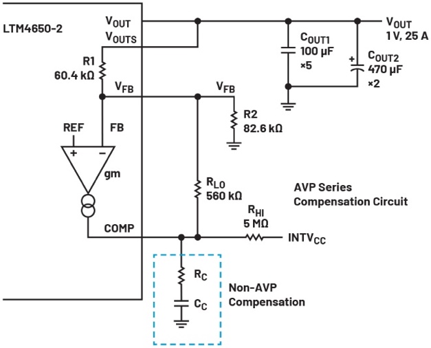
Figure 4. Circuit employing AVP (series compensation circuit).
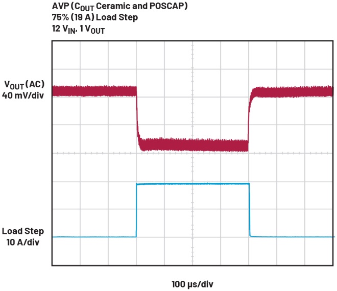
Figure 5. Load transient waveform for the circuit employing AVP (Figure 4), with an output voltage transient of 95 mV peak-to-peak. COUT1 = 5 × 100 μF ceramic capacitor, COUT2 = 2 × 470 μF POSCAP capacitor.
When implementing the AVP solution, the two POSCAPs may be substituted with two ceramic capacitors, thus utilising a total of seven 100 μF ceramic capacitors on COUT1. The advantages of using ceramic capacitors include lower equivalent series resistance (ESR) and equivalent series inductance (ESL), reduced cost, smaller size, and more reliable performance. Transient performance has been improved, with measured results showing VOUT at 104 mV peak-to-peak, as illustrated in Figure 6.
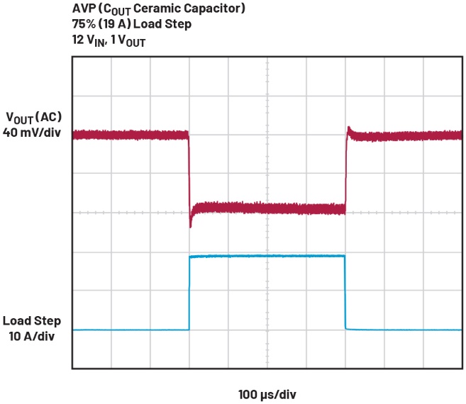
Figure 6. Load transient waveform for the circuit employing AVP, with an output voltage transient of 104 mV peak-to-peak. COUT1 = 7 × 100 μF ceramic capacitor.
Table 1 displays the load transient response V p-p for the aforementioned measurements: non-AVP (baseline), AVP, and AVP using only the output ceramic capacitor, for comparison.
Table 1. Comparison of load transient response V p-p between non-AVP, AVP, and AVP using only the output ceramic capacitor.
|
|
非AVP
|
AVP
|
AVP
|
|
|
5× 100 μF
|
5× 100 μF
|
7× 100 μF
|
|
|
陶瓷电容
|
陶瓷电容
|
仅陶瓷电容
|
|
|
+ 2× 470 μF POSCAP
|
+ 2× 470 μF POSCAP
|
|
|
负载瞬态响应,V p-p (mV)
|
136
|
95
|
104
|
Conclusion
Implementing an AVP series compensation circuit on the LTM4650-2 μModule regulator not only enhances transient response performance but also reduces load power dissipation under high load conditions. The output capacitance requirement is less than 50%. Consequently, ceramic capacitors may be substituted for POSCAPs, thereby reducing costs and minimising occupied PCB space. This AVP circuitry is also applicable to numerous other μModule regulators featuring external compensation pins and external RC compensation networks (e.g., LTM4630-1, LTM4626, LTM4636, LTM8055-1, etc.).

 English