Many applications in data centres, artificial intelligence (AI) and communications utilise multi-phase buck regulators with a 12 V input voltage. Figure 1(a) depicts a conventional 8-phase buck converter, where discrete inductors (DL) are arranged in a row with a spacing typical in the industry of 8.3 mm per phase. Figure 1(b) illustrates an alternative solution employing the same layout, where the discrete magnetic components are replaced by two 4-phase coupled inductors (CL).
The question arises: why would a customer choose this alternative? And what motivated ADI to develop this unique solution—merely to stand out? The answer lies in the significantly enhanced figure of merit (FOM) of the CL configuration, which can be tailored to different customer priorities. The common-frame (CF) strategy ensures identical footprints for all devices. Thus, when solution sizes are comparable, optimisation efforts focus on enhancing efficiency.
For DL and CL, their fundamental principles and key distinctions should be considered. The current ripple in each phase of a conventional buck converter can be calculated using Equation 1, where the duty cycle is D = VO/VIN, VO is the output voltage, VIN is the input voltage, L is the inductance value, and Fs is the switching frequency.
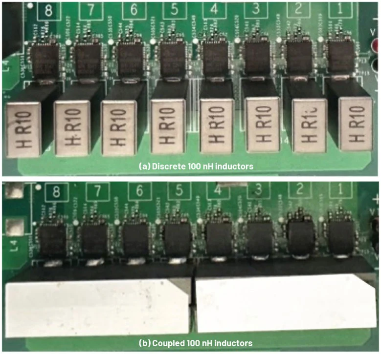
Figure 1.8 Phase-shifted buck regulator, with a spacing of 8.3 mm per phase, featuring (a) discrete inductors and (b) two 4-phase coupled inductors.
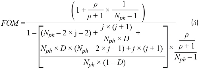
Alternatively, the current ripple in a coupled inductor with leakage inductance Lk and mutual inductance Lm may be expressed by Equation 2.1. The Figure of Merit (FOM) is represented by Equation 3, where Nph denotes the number of coupled phases, ρ is the coupling coefficient (Equation 4), and j is the operating index defining the applicable duty cycle range (Equation 5).
Comparing Equations 1 and 2 reveals that FOM is the primary distinguishing factor, demonstrating CL's superiority over DL in current ripple elimination. The FOM value depends on multiple factors, and in CL, it can typically be substantially higher, signifying a significant performance improvement. However, the FOM advantage alone does not guarantee a large performance differential. The system must consciously leverage the benefits of increased FOM according to the required priorities.
CL optimisation
Commencing with the reference design from VIN = 12 V to VO = 1 V, wherein DL = 100 nH provides baseline performance, the CL FOM for the Nph = 4 building block is plotted for several practically reasonable values of the coupling ratio Lm/Lk, as shown in Figure 2. The red curve for Lm/Lk = 0 represents the baseline FOM = 1 for discrete inductors. Here, the objective is to maintain identical transient performance and an identical output capacitance slot Co, hence selecting the same 100 nH value for CL leakage. As demonstrated in the article ‘Addressing Core Loss in Coupled Inductors’² and the video ‘Fundamentals and Advantages of Coupled Inductors’¹, and clearly visible in Figure 2, ideally the Lm value should be maximised to achieve the highest coupling coefficient (Equation 4), thereby increasing the FOM. Within the given dimensions (h = 12 mm, phase pitch 8.3 mm/phase), a reasonable Lm = 260 nH is achievable with an extremely conservative Isat = 25 A, which relates to the permissible phase-to-phase current imbalance. Note that the load capability of CL is defined by Lk's Isat, which in this CL design exceeds the DL Isat rating at >100 A per phase (at 105°C).
The duty cycle range for 12 V to 1 V applications corresponds to D ~ 0.083. For a conservative Lm/Lk ratio of 2.6, the Figure 2 shows FOM > 2.5, indicating that the CL's Fs can be readily halved to maintain low current ripple. As several losses proportional to switching frequency would decrease, this should significantly improve efficiency.
Increasing Lm typically favours current ripple reduction, yet Figure 3 demonstrates that Lm = 260 nH achieves most current ripple elimination benefits without diminishing returns (where further increases yield marginal improvement).
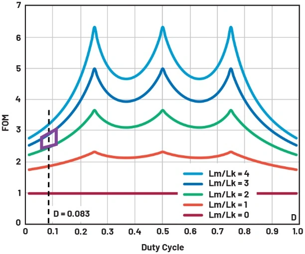
Figure 2. Function relationship between the figure of merit (FOM) of a four-phase CL and duty cycle D for various Lm/Lk values. The target region is highlighted.
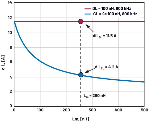
Figure 3. Current ripple versus Lm as a function of DL = 100 nH and CL = 4 × 100 nH, under conditions of VIN = 12 V, VO = 1 V, and Fs = 800 kHz.
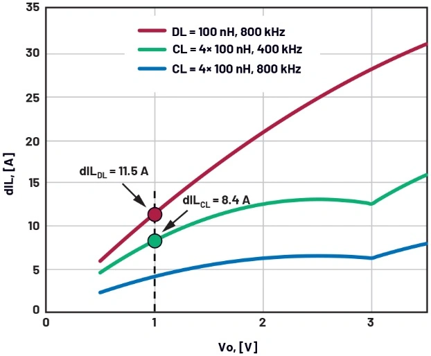
Figure 4. Current ripple versus output voltage (VO) at VIN = 12 V, with DL = 100 nH (800 kHz) and CL = 4 × 100 nH (800 kHz, 400 kHz).
Figure 4 plots the corresponding current ripple, comparing the baseline design DL = 100 nH under VIN = 12 V and Fs = 800 kHz conditions with the proposed four-phase CL = 4 × 100 nH (Lm = 260 nH). Evidently, the CL solution can operate at Fs = 400 kHz rather than 800 kHz, yet still exhibits lower current ripple compared to DL = 100 nH at 800 kHz. The reduced peak-to-peak ripple implies lower root mean square (RMS) values for all circuit waveforms, including conduction losses. The primary efficiency gain stems from halving Fs, substantially reducing switching losses, dead-time losses in the FET body diode, reverse recovery, and gate drive losses. Note that the most pronounced efficiency gains occur under light load conditions where AC losses are more pronounced. However, certain losses (such as voltage and current overlap during switching transitions) scale proportionally with load current, meaning efficiency improvements will also be evident at full load.
The developed 4× 100 nH coupled inductor is shown in Figure 5. Note that the pinout complies with DL space requirements and is compatible with multiple sources and alternatives.
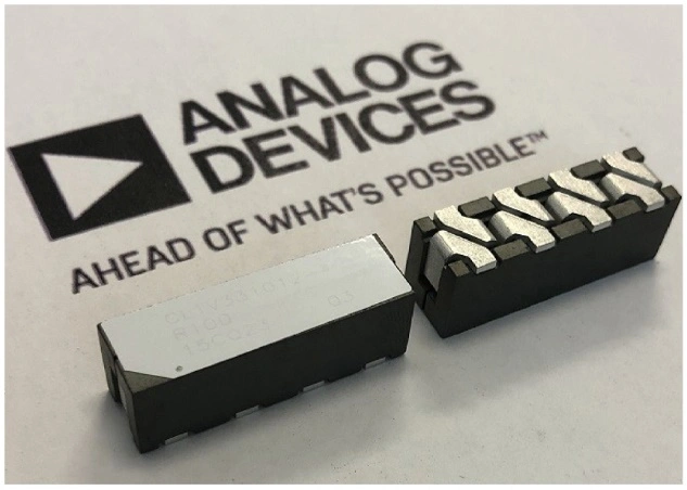
Figure 5. Developed CL = 4 × 100 nH, 33.5 mm × 10 mm × 12 mm.
Experimental results
The transient performance of the four-phase buck converter is shown in Figure 6, comparing waveforms for an 8-phase configuration with DL = 100 nH (600 kHz) and a 2× CL = 4× 100 nH (400 kHz) configuration. As anticipated, identical current slew rates and matching output capacitance yield comparable transient performance. Since a transient change in the duty cycle of one phase causes simultaneous current variations across all phases, the coupled phases effectively augment the phase margin of the feedback loop. This, combined with the multi-phase topology, mitigates the potential reduction in feedback bandwidth resulting from the decreased CL switching frequency.
Figure 7 displays corresponding efficiency comparisons at different switching frequencies, where dashed lines represent DL and solid lines denote CL. At high switching frequencies, both CL and DL exhibit negligible current ripple, resulting in comparable efficiency. However, owing to CL's distinct current ripple advantage, reducing CL's Fs substantially decreases overall losses without significant impact from increased current ripple. The efficiency of the DL solution also improves with decreasing Fs, but at a progressively slower rate. This is because excessive current ripple degrades the root mean square (RMS) value of the waveform, leading to non-linear increases in core losses and ACR losses. Consequently, CL exhibits a clear efficiency advantage over DL: 1% at peak and 0.5% at full load. Corresponding thermal performance is also improved.
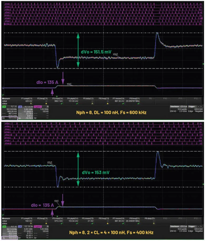
Figure 6.135 Transient performance under load step A, with VIN = 12 V and VO = 0.9 V, for 8-phase DL = 100 nH (600 kHz) and 2× CL = 4× 100 nH (400 kHz). Same PCB, same Co, same conditions.
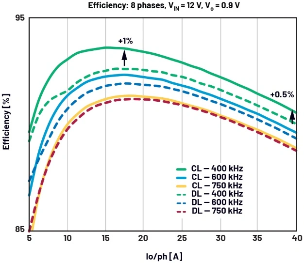
Figure 7.8 Comparison of measurement efficiency between a design with DL = 100 nH (dashed line) and one employing a unified packaging strategy with 2× CL = 4× 100 nH (solid line), VIN = 12 V, VO = 0.9 V.
In accordance with the Common Package (CP) strategy, the CL solution designed to replace discrete inductors employs identical footprint and overall dimensions, serving as a 4-phase building block for applications ranging from 12 V to ~1 V. By leveraging the advantages of CL, efficiency is significantly enhanced whilst maintaining transient performance. Experimental results validate the design and optimisation strategy based on Figure of Merit (FOM).
The overall performance improvement achieved demonstrates the superiority of ADI IP in coupled inductors.

 English










