A switching power supply with sufficiently low noise levels to directly power noise-sensitive components
A switching power supply with sufficiently low noise levels to directly power noise-sensitive components
December 15 , 2025
Posted by KUKE
0
Have you encountered situations where the output results of an ADC exhibit slight deviations and random variations? This may be caused by noise within the ADC system itself. A common source of noise is the power supply rail for the voltage-controlled oscillator (VCO). Noise on this supply rail can introduce jitter to the clock signal, which is subsequently used as the sampling clock for the ADC. Significant jitter may introduce errors in ADC conversions, leading to erroneous data.
It is well known that Switching Mode Power Supplies (SMPS) require switching operations during voltage conversion, inevitably generating noise. Employing an SMPS for the clock supply rail introduces this noise into the ADC system. To minimise errors, noise-sensitive components are typically powered by Low Dropout (LDO) regulators with noise suppression capabilities.
ADI's LTM8080 buck regulator SMPS device integrates a post-regulator dual LDO regulator with noise suppression technology. Similar to the standalone LT3045 LDO regulator, this SMPS device delivers low-noise power rails.
Why is it essential to monitor power rail noise?
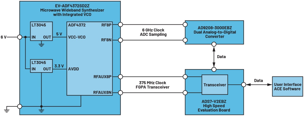
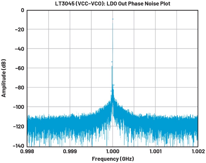
Power rail noise is a critical factor capable of significantly impacting system performance. In Figure 1, the LT3045 LDO regulator serves as a low-noise power rail, supplying the VCO of the ADF4372 frequency synthesiser. The ADF4372 then generates clock signals for the AD9208 ADC and the FPGA board. Figure 2 displays the phase noise plot obtained from the output of the LT3045 LDO regulator, which serves as a benchmark for comparing alternative power rail solutions.
Figure 1. Basic Block Diagram of VCO/ADC Configuration
Figure 2. LT3045 phase noise diagram as a reference (1 GHz, 2 MHz sweep)
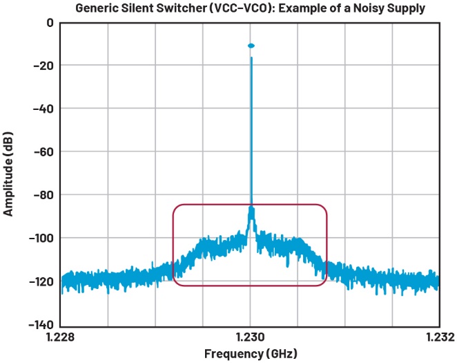
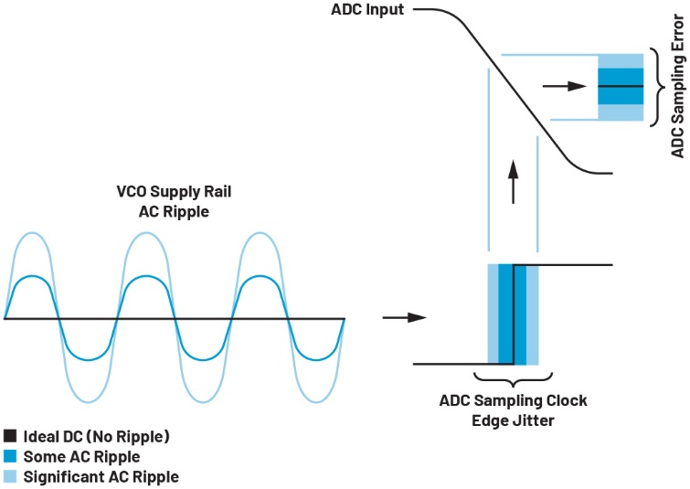
Compared to the baseline design, employing a higher-noise power rail yields a less favourable noise spectrum, as illustrated in Figure 3, where the sidebands exhibit a slight elevation. When these sidebands reach a certain threshold, they introduce jitter to the rising edge of the ADC sampling clock (Figure 4). Consequently, the ADC samples the analogue input signal at unintended time points, resulting in anomalous data words containing bit errors.
The occurrence of bit errors may have significant consequences, particularly when the errors are severe. The deviation between the actual data word from the ADC and the expected data word may trigger unexpected system behaviour. For instance, if the data word indicates an input voltage higher than the actual voltage, the device may be prematurely activated before the system is prepared. In safety-critical applications, such an unintended state could lead to the disabling of safety features.
Figure 3. Illustrative phase noise diagram for a high-noise SMPS (1.23 GHz, 2 MHz bandwidth)
Thanks to EMI noise shielding technology, the SMPS can now be positioned near the LDO regulator without coupling switching noise to the LDO's output. Packaging the SMPS and LDO regulator together offers additional benefits beyond noise reduction. See Table 1.
Advantages of integrating switch-mode buck converters and LDO regulators within a single package
Table 1. Advantages of SMPS + LDO Regulators Compared to Standalone LDO Regulators
Design characteristics
Switching Mode Power Supply + LDO Voltage Regulator
LDO voltage regulator
Input power flexibility
Wide input range (3.5 V to 40 V)
Narrow input range
Standard input voltage rail
Unique input voltage rail
PCB layout is straightforward
Noise-sensitive wiring is located within the device.
Special cabling is required to minimise noise as far as possible.
Only basic PCB layout skills are required.
More advanced PCB routing techniques are required.
The device may be placed near other noise-sensitive components.
Save PCB space
Direct voltage conversion from 12 V/24 V supply rails to LDO regulator output voltage
An additional voltage regulator may be required to
No uncommon intermediate bus voltage required
12 V/24 V power supply rails converted to a specific intermediate bus voltage
Simple design
The design has been thoroughly tested and optimised.
Further preliminary design/testing is required to minimise noise as much as possible.
Users can plug and play
Potential system efficiency improvements
Lower parasitic losses
Optimised LDO regulator margin
The step-down regulator section can directly supply power to other external LDO regulators.
A device integrating a buck converter (SMPS) with an LDO regulator offers multiple advantages. It can be powered from standard supply rails such as 12 V or 24 V, providing considerable input power flexibility. Furthermore, an intermediate bus can be designed to maintain a specific voltage above the LDO regulator's output, ensuring stable operation even when the device is supplied from a higher voltage source. This “voltage input to output control” (VIOC) feature ensures the LDO regulator maintains its specified margin by regulating the upstream SMPS output. VIOC is indispensable for preserving power supply rejection ratio (PSRR) whilst enhancing efficiency.
The combination of SMPS and LDO regulator permits noise-sensitive routing to be implemented within the device's internal circuitry. Consequently, basic routing techniques at the PCB level suffice to optimise the device's noise performance.
Furthermore, thanks to fully integrated EMI noise shielding, noise from the on-chip SMPS is not radiated omnidirectionally but is directed away from the LDO regulator. This technology permits the placement of the switching regulator near the LDO regulator without compromising the latter's noise suppression capability. Consequently, this fully integrated device can be deployed in areas previously unsuitable for SMPS placement due to noise concerns.
Should the SMPS section of the device provide current exceeding the LDO regulator's rating, multiple LDO regulators may be integrated within the package. Furthermore, external LDO regulators may be connected to an intermediate bus, thereby offering greater design flexibility to the user.
To ensure compliance with specifications outlined in the device data sheet, this fully integrated SMPS plus LDO regulator combination has undergone comprehensive testing to guarantee it meets stipulated requirements.
Switching buck converters with noise levels as low as LDO regulators
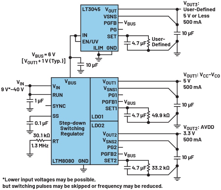
Compared to a reference LDO regulator solution, the LTM8080 offers greater input supply voltage flexibility and lower power dissipation. Figure 5 illustrates an example solution employing the LTM8080, demonstrating design flexibility. Integrated with the co-packaged buck regulator and LDO regulator, the LTM8080 incorporates EMI noise shielding that effectively directs the propagation path of radiated noise.
Figure 5. The LTM8080 solution replaces the two LT3045 LDO regulators on the ADF4372SD2Z evaluation board and supports an optional user-defined third LDO regulator output for greater system flexibility.
Comparing the noise suppression capabilities of the LTM8080 and LT3045, the measurement results are almost identical. Table 2 presents the SNR comparison results, whilst Figure 6 displays the phase noise plots. Consequently, the LTM8080 serves as a viable alternative to the LT3045, effectively reducing bit errors whilst providing excellent noise suppression.
Table 2. SNR Comparison: LTM8080 versus LT3045
ADF4372: 5 V PLL Clock Power Supply
SNR:AD9208
LT3045
(Benchmark)
53.6 dBFS
LTM8080
53.6 dBFS
Figure 6. Phase noise diagram: LTM8080 (left) versus LT3045 (right)
Test results clearly demonstrate that SMPS devices incorporating advanced noise suppression techniques (such as EMI noise shielding) can effectively replace LDO regulators for powering noise-sensitive supply rails. Although the proof-of-concept primarily targeted VCO supply rails, the design flexibility afforded by solutions integrating SMPS and LDO regulators can also benefit numerous other noise-sensitive applications.

 English