Introduction
The primary innovation of this switch lies in its ingenious integration of passive components and independently controlled switching with a Serial Peripheral Interface (SPI). By incorporating resistors and capacitors directly into the switch package, designers achieve significant space savings. This design architecture substantially reduces PCB footprint by up to 80%, making it ideal for applications with extremely stringent space constraints.
The pass-through pin feature delivers a revolutionary solution for PCB designers. This capability permits SPI and power traces to traverse the switch routing directly and efficiently, eliminating the need for additional vias or complex routing configurations. This simplified approach not only reduces design complexity but also substantially increases switch channel density, enabling the creation of more compact, higher-performance designs.
Beyond space savings, this switch exhibits exceptionally low on-resistance of approximately 0.5 Ω. This characteristic is crucial for enhancing measurement accuracy and effectively reducing thermal generation when handling high currents. With its low on-resistance, the device delivers outstanding signal integrity and precision across diverse applications, including automated test equipment and precision measurement and control systems. Furthermore, the low on-resistance improves thermal resistance, ensuring reliable and consistent performance even under varying environmental conditions.
Challenges in Maximising Channel Count
When designing systems with the objective of maximising channel count, PCB space becomes a precious resource. Switches play a vital role in increasing system channel numbers, but as the number of switches increases, PCB space is occupied not only by the switches themselves but also by the logic control lines and associated passive components required for their proper operation. Consequently, the additional components needed to control the switches consume significant space, resulting in a reduction in the achievable channel count.
Traditional Switching Solutions
A common approach to increasing channel density involves employing switches controlled via an SPI logic interface, such as the eight-channel SPI switch ADG1414. This architecture offers distinct advantages over parallel interfaces, requiring only four GPIO lines for implementation and utilising just one SPI port on a standard microcontroller. For systems incorporating numerous switches, the daisy-chain functionality provided by the device can be leveraged to control all units simultaneously. Figure 1 illustrates an example of 25 ADG1414 devices configured in daisy-chain mode to control 200 LEDs. Additionally, three decoupling capacitors and one pull-up resistor are required to ensure proper circuit operation. This implementation necessitates the placement of 125 components, occupying approximately 2600 mm² of PCB area.
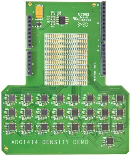
Figure 1. Example PCB layout featuring 25 ADG1414 devices
Advanced Packaging
By directly integrating passive components into the switch package (as shown in Figure 2), designers can achieve significant space savings. The ADGS2414D incorporates decoupling capacitors for the VDD, VSS, and RESET/VL power pins, eliminating the need for external decoupling capacitors. The pull-up resistor for the SDO pin is also integrated. Combined with the multi-chip stacking of the switch circuitry, this significantly reduces the overall size of the switch, which is housed in a 4 mm × 5 mm LGA package.
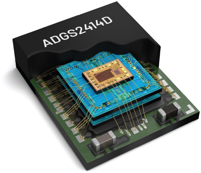
Figure 2. ADI's innovative stacked three-chip solution
Through-Pins
When multiple devices are employed within a system, the through-pin feature enables more compact layouts and increased channel density. This capability facilitates seamless transmission of power and digital lines between devices. Both the top and bottom pins of the package provide VDD, RESET/VL, and GND power lines, alongside SCLK, CS, SDI, and SDO digital lines. Through-pin functionality simplifies PCB routing and reduces the need for vias when connecting multiple devices. Figure 3 illustrates a PCB layout example where four ADGS2414D devices configured in a daisy-chain arrangement utilise the through-pin feature, significantly reducing the overall footprint of the layout.

Figure 3. Example of PCB layout utilising through-hole pin characteristics
ADI Switching Solutions
As previously outlined, the conventional switching solution depicted in Figure 1 necessitates the placement of 125 components, occupying approximately 2600 mm² of PCB area. By leveraging innovative passive component co-packaging and the pass-through pin characteristics of the eight-channel switch, a novel PCB design achieving significantly enhanced density can be realised. Figure 4 illustrates the same application scenario, where 25 ADGS2414D switches control 200 LEDs. Utilising daisy-chain functionality, all devices can be controlled simultaneously. Notably, this layout eliminates passive components, allowing switches to be densely packed with typical spacing of 1 mm between devices on adjacent sides. This design requires only 25 devices, occupying approximately 800 mm² of PCB area – a 70% reduction. Beyond saving PCB area, the elimination of 100 passive components substantially reduces manufacturing costs while enhancing product quality and reliability.
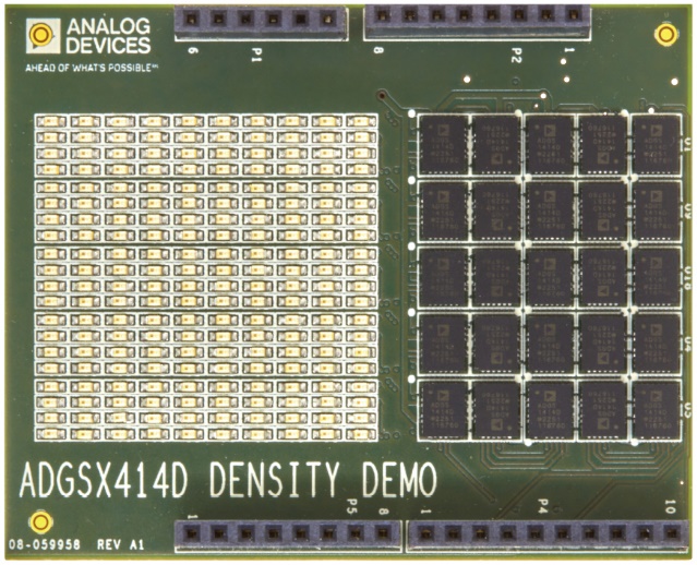
Figure 4. Example PCB layout with 25 components
Low On-Resistance
Beyond its space-saving design, the ADGS2414D boasts an outstanding low switch on-resistance, typically 0.5 Ω. This low resistance minimises voltage drop (I×R) within the measurement signal chain, thereby enhancing overall system-level accuracy. In high-channel-density applications, greater precision translates to reduced channel-to-channel variation and less frequent calibration, ultimately lowering costs and improving product test yield.
This switch can handle significantly higher switching currents, up to 850 mA per channel. This capability proves particularly crucial when managing high-current switching scenarios. Furthermore, managing heat generated by power dissipation within the switches is vital, especially in high-channel-density applications where thermal management can pose significant challenges. Here, the low on-resistance proves advantageous once more, as the power lost as heat (I² × R) is substantially reduced due to the low resistance. This characteristic ensures stable internal system temperatures and helps prevent overheating issues.
Daisy Chain Configuration
The ADGS2414D supports connecting multiple devices via a daisy chain configuration, as illustrated in Figure 5. In this setup, all devices share the same CS, SCLK, and VL lines. The SDO of one device connects to the SDI of the next, forming a shift register. A single 16-bit SPI frame command drives all devices in the daisy chain into Daisy Chain Mode. Within this mode, the SDO is an 8-cycle delayed version of the SDI, enabling the desired switch configuration to propagate sequentially from one device to the next along the chain.
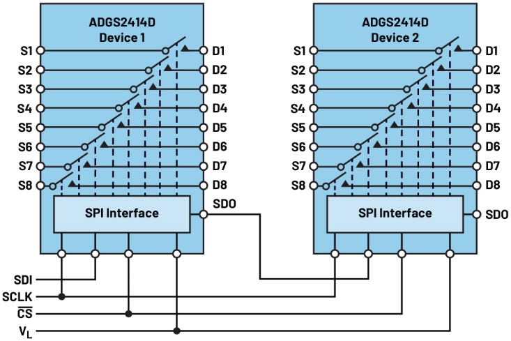
Figure 5. Two ADGS2414D devices in a daisy chain configuration
Error Detection Functionality
Protocol errors and communication errors on the SPI interface can be detected. Three types of error detection are available: SCLK count error detection, invalid read/write address error detection, and CRC error detection. Each error detection function may be enabled or disabled using the corresponding enable bit within the error configuration register. Furthermore, within the error flag register, each error detection function possesses a corresponding error flag bit.
Conclusion
The ADGS2414D delivers a breakthrough solution for PCB design and electronic measurement technology. Featuring innovative passive component co-packaging, through-pin functionality, an SPI interface, and low on-resistance, it significantly reduces board footprint, increases channel density, and enhances measurement accuracy. Utilising a multi-chip package, it inherits the outstanding switching performance of ADI's current switching products. The introduction of this device marks the arrival of an innovative precision switching solution capable of substantially increasing switching channel density.

 English