Abstract
This article constitutes the second part of a two-part series on Voltage Input to Output Control (VIOC) applied to Low Dropout Regulators (LDOs). Building upon the fundamental concepts introduced in Part One, it delves into the design of VIOC systems and elucidates how the latest generation of LDOs maintain a constant input-output voltage difference. This approach delivers critical performance advantages, including enhanced Power Supply Rejection Ratio (PSRR), optimised power dissipation, and robust fault protection. The article highlights the ease of implementing VIOC through reference designs and straightforward evaluation methods, including LTspice® simulation and demonstration hardware. It also explores integrating VIOC within negative voltage topologies and reviews earlier VIOC implementations, including those utilising discrete components and conventional LDO architectures. By simplifying the collaboration between switching regulators and LDOs, VIOC enhances circuit performance and offers flexible solutions for modern power management systems.
Introduction
In the first part of this series, an initial introduction was provided to the voltage input-to-output control (VIOC) feature within the latest generation of low-dropout regulators (LDOs), whilst the second instalment will delve deeper into its functionality. To facilitate engineers' grasp of VIOC system design, this article also offers readily available reference designs and straightforward evaluation methodologies. Furthermore, it explores how VIOC can be seamlessly implemented within negative voltage topologies, thereby broadening its scope of application. Concurrently, the article traces the evolutionary path of early VIOC implementations to furnish essential historical context.
VIOC Explained
The VIOC feature in the latest generation of LDOs is implemented via an internal differential amplifier with unity gain, as illustrated in Figure 1. The schematic of the differential amplifier reveals its composition of an operational amplifier and discrete resistors. In its most fundamental configuration, the differential amplifier's output is directly connected to the feedback (FB) pin of the switching regulator powering the LDO. The connection between the VIOC and FB pins forms a closed-loop feedback circuit. Within this circuit, the switching regulator outputs a voltage higher than the LDO output by an amount equal to the differential amplifier's output voltage. This differential amplifier output voltage is connected to the switching regulator's FB pin. The FB pin serves as the external connection point for the inverting input of the switching regulator IC's error amplifier.
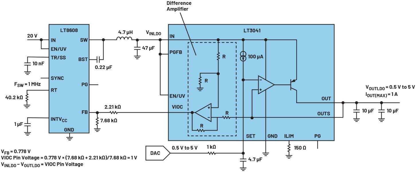
Figure 1. The VIOC characteristic in the latest generation of LDOs is achieved through an internal differential amplifier with a gain of one.
An error amplifier is an electronic component, typically implemented using an operational amplifier, whose function is to amplify the difference between two input signals (usually a reference voltage and a feedback signal from the system output). This difference (the error signal) is used to adjust the system to maintain the desired output. Consequently, error amplifiers are a critical component in feedback control systems such as voltage regulators, power supplies, and servo mechanisms.
The differential amplifier implementing VIOC also handles certain management tasks, such as preventing LDO input undervoltage and shutting down the LDO. For comprehensive details on VIOC behaviour, refer to the VIOC section within the LDO data sheet.
The voltage at the FB pin of a switching regulator typically ranges from approximately 0.4 V to 1.2 V, depending on the switching regulator IC. If the voltage at the switching regulator's feedback pin falls below the required LDO input-output voltage difference, a resistor may be added between the switching regulator's FB pin and the LDO's VIOC pin. This resistor connects the VIOC signal at the differential amplifier's output to a higher voltage point, as illustrated in Figure 1. As demonstrated in Figure 1 for the LT3041 LDO and similar LDOs, achieving an LDO input-output voltage difference lower than the switching regulator's FB pin voltage is challenging.
To understand how the differential amplifier implements VIOC, consider its output as one of its inputs. If the differential amplifier's output voltage is a specific value, the voltage at its positive input must be higher than that at its negative input, with the difference equal to the differential amplifier's output voltage. The differential amplifier's negative input is connected to the LDO's output. Consequently, the differential amplifier regulates the switching regulator's output voltage to be higher than the LDO's output voltage by an amount equal to the differential amplifier's output voltage (determined by the switching regulator's FB pin voltage).
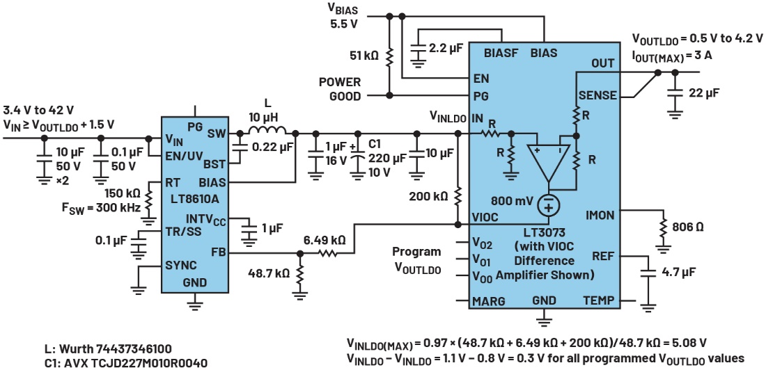
Figure 2. The LT3073 LDO incorporates a VIOC circuit design that enables the LDO's input-output voltage difference to be lower than the feedback pin voltage of the switching regulator, thereby limiting the output voltage of the LT8610A switching regulator.
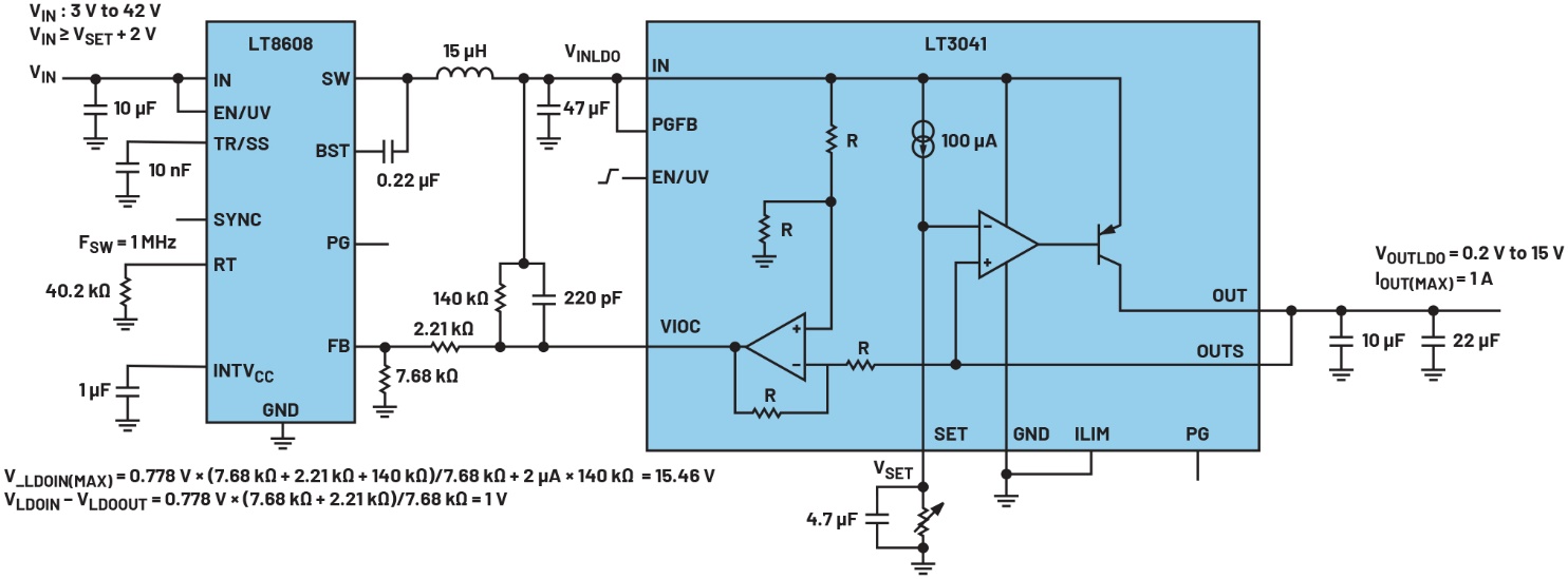
Figure 3. If the LDO is not enabled, the LT3041 VIOC circuit will limit the output voltage of the LT8608 switching regulator.
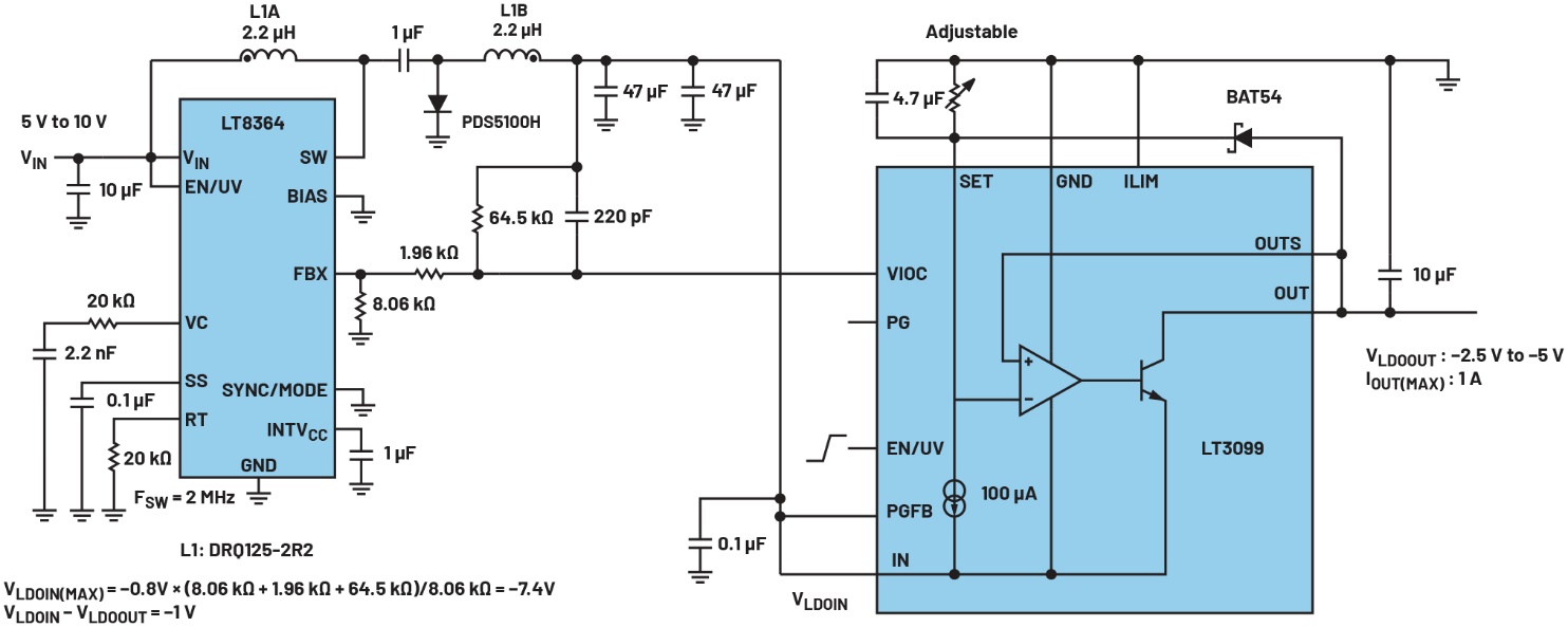
Figure 4. Switching regulator employing a Ćuk configuration for generating negative voltages (using the LT8364)
Figure 2 illustrates the LT3073 LDO featuring a VIOC circuit design that enables the LDO's input-output voltage difference to be lower than the feedback pin voltage of the switching regulator. This VIOC approach provides a bias voltage, resulting in an LDO input-output voltage difference that is 800 mV lower than the VIOC pin voltage. This type of VIOC is commonly found in LDOs with lower input-output voltage differences and higher current ratings. The circuit in Figure 2 also limits the output voltage of the switching regulator. The feedback resistor divider in the switching regulator prevents its output voltage from becoming excessively high when the LDO is disabled or unable to close the VIOC feedback loop. As shown in Figure 3, the LT3041 VIOC circuit in Figure 1 limits the output voltage of the switching regulator LT8608.
The LDOs discussed thus far are positive LDOs operating with positive voltages, but VIOC operation also supports negative LDOs operating with negative voltages. The VIOC circuit for a negative LDO can be implemented using a switching regulator that generates a negative voltage, with its feedback pin designated as FBX rather than FB. Figure 4 shows a switching regulator in a Ćuk configuration used to generate a negative voltage. The VIOC of the negative LDO LT3099 is employed to control the Ćuk output voltage.
The circuit depicted in Figure 5 illustrates an increasingly common scenario where a buck regulator, typically generating positive voltage, is configured as an inverted buck-boost regulator to produce negative voltage. As standard buck regulators lack an FBX or FB pin suitable for negative voltage operation, this VIOC circuit requires a level shifter. In this circuit, the level shifter forms part of the circuitry, comprising an LT1636 operational amplifier and a network connected to the positive input of the op-amp.
Implementing VIOC is straightforward, requiring merely the addition of a single wire to the existing switch-mode regulator-to-LDO connection. VIOC can be used with any switch-mode regulator featuring an FB pin. Note that Silent Switcher® 3 (SS3) regulator ICs lack an FB pin, so VIOC is not typically employed with these devices. VIOC imposes certain limitations when the switching regulator's FB pin connects to an internal resistor network that also links to the output. This scenario applies to certain μModule® regulators.
μModule regulators represent a highly integrated System-in-Package (SiP) solution, integrating multiple electronic components within a compact package. These include the DC-DC controller, power transistors, input and output capacitors, compensation components, and inductors.
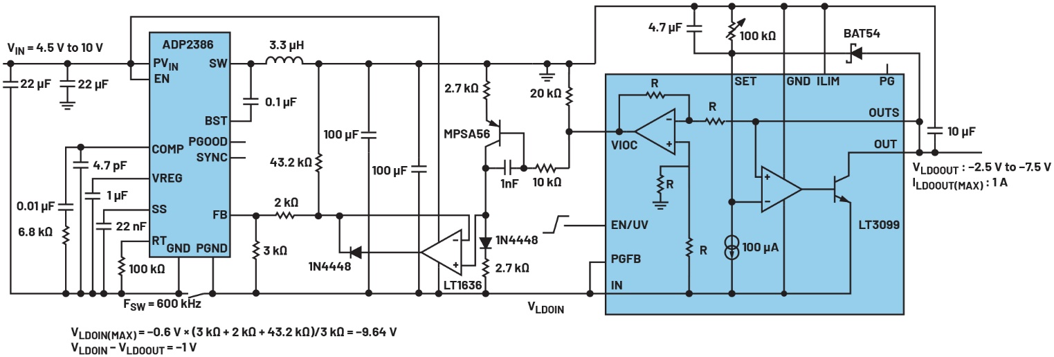
Figure 5. If the switching regulator employs an inverted buck-boost configuration (using the ADP2386), the VIOC circuit for the negative LDO requires a level shifter.

Figure 6. This VIOC circuit pairs one channel of the LTM4616 μModule regulator with the LT3078 LDO.
The VIOC circuit shown in Figure 6 combines one channel of the LTM4616 μModule regulator with the LT3078 LDO. An internal 10 kΩ resistor connects the μModule's FB pin to the output of the switching regulator. The current flowing through the VIOC pin (and the corresponding voltage at the VIOC pin) is proportional to the current through the 10 kΩ resistor; this resistor current changes proportionally as the output voltages of both the LDO and the switching regulator increase or decrease. This dependency of the VIOC pin voltage on the LDO output voltage limits the LDO output voltage regulation range in the circuit shown in Figure 6.
A convenient method for evaluating the operational status of the VIOC system
LTspice® can be employed for rapid simulation and evaluation of VIOC operation within constrained environments, thereby enabling testing of diverse scenarios and parameters without physical hardware. Consequently, it serves as an effective tool for verifying circuit behaviour and optimising designs prior to circuit implementation.
The most efficient method for evaluating VIOC functionality using hardware involves connecting the switching regulator demonstration circuit to the LDO demonstration circuit with minimal modifications. Figure 7 illustrates two such configurations for rapid VIOC testing. For the final design of a VIOC circuit, load transient testing on actual hardware is typically required to verify circuit stability. To enhance stability, capacitance is commonly added at the switching regulator output. For guidance, refer to the VIOC reference design in the data sheet.

Figure 7. Two demonstration circuits enabling rapid testing of VIOC operation with minimal modifications (using DC3158A and DC2458A)
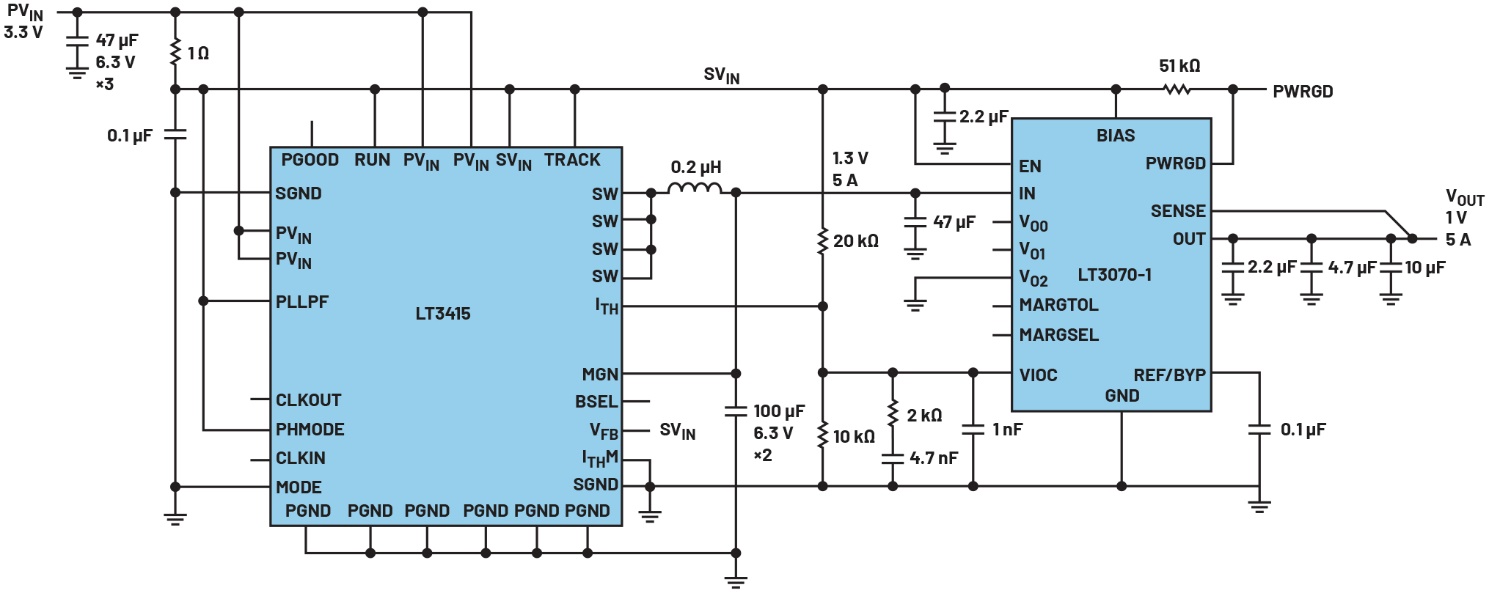
Figure 8. An early version of the VIOC (using the LTC3415)
Early-generation VIOC and non-integrated VIOC
Thus far, most discussion has centred on LDOs employing the latest generation of VIOC. Beyond this, an alternative approach utilises discrete components to implement VIOC functionality, employing earlier-generation LDOs featuring VIOC characteristics. Figure 8 illustrates an LDO circuit employing an early-generation VIOC. The LDO's VIOC pin connects to the switch-mode regulator's ITH or VC pin, with the LDO's VIOC circuit automatically maintaining the input-output voltage difference around 300 mV. The ITH or VC pin serves as the external connection point for the switch-mode regulator IC's error amplifier output. Early 5V, 5A LDOs, such as the LT3070-1 and LT3071, and LT3072, employed this VIOC approach.
The final category of VIOC we shall discuss is that implemented using discrete components. With discrete components, VIOC functionality can be added to almost any LDO. This method was particularly prevalent in early current-source reference LDOs (beginning with the LT3080), as altering the output voltage of an LDO with a current-source reference via an external voltage signal or digital potentiometer is relatively straightforward. A current source reference LDO is a regulator that employs a current source to drive a resistor, thereby determining the output voltage, rather than utilising a reference voltage source. Figure 9 illustrates a circuit implementing VIOC using discrete components. The source-gate voltage of the IRF7342 PMOS determines the input-output voltage difference of the LDO. For further reference designs employing this type of VIOC, please consult the LT308x data sheet.
Figure 9. Circuit implementing VIOC using discrete components LT8646S and LT3083
Conclusion
The integration of LDOs and switching regulators using VIOC technology offers significant advantages for modern power management designs. VIOC maintains a stable input-output voltage difference, thereby enhancing PSRR to reduce output noise, improving power efficiency, and strengthening fault protection and start-up reliability. It also ensures stable load transient response, which is critical for high-performance systems.
VIOC simplifies voltage coordination between the switching regulator and LDO, optimising the design process and improving overall circuit efficiency. The latest generation of VIOC-enabled LDOs provides flexible, high-performance solutions for today's complex electronic applications.
To expedite the design process, explore the detailed application notes, reference designs, and LTspice simulation models available at analog.com. Leveraging simulation tools enables testing and optimisation of circuits prior to hardware implementation, thereby saving time, mitigating risks, and achieving greater levels of innovation.

 English