Linear Voltage Regulator Input-to-Output Control – Part One Quick Start and Advantages
Linear Voltage Regulator Input-to-Output Control – Part One Quick Start and Advantages
February 16 , 2026
Posted by KUKE
0
Abstract
This two-part series introduces voltage input-to-output control (VIOC) systems. Such systems are typically configured as combinations of low-dropout (LDO) regulators with VIOC characteristics and buck topology switching regulators. Subsequently, the article provides specific guidance for VIOC system design, including a recommended pairing list for LDOs and switching regulators, alongside explanations for the rationale behind these pairings. Finally, it demonstrates how the VIOC capability of the LDO can be leveraged to reduce noise at the LDO output, optimise power dissipation, protect the system during faults, and ensure reliable operation under dynamic conditions such as start-up and overload. Part Two builds upon Part One, delving deeper into VIOC system design and providing an overview of the operating principles and background of VIOC.
Introduction
Within power management, low-dropout (LDO) regulators play a pivotal role in ensuring electronic components receive high-performance power. The low-noise performance of LDOs is critical, particularly in noise-sensitive applications such as precision analogue circuits, RF systems, and medical equipment, where LDOs deliver clean power, effectively reducing interference and enhancing signal integrity. When integrated with Voltage Input to Output Control (VIOC) functionality and compatible switching regulators, LDOs form systems that perpetually maintain optimal input-output voltage differentials. This design not only substantially reduces noise and achieves high Power Supply Rejection Ratio (PSRR) but also ensures efficient, protected, and robust system operation. This article delves into the intricate details of implementing VIOC, elucidating its advantages and practical applications. By understanding the synergistic effects of VIOC, engineers can optimise power management solutions for diverse electronic devices.
Whether incorporating VIOC or not, LDOs fall within the power management product category. Power management involves utilising integrated circuits (ICs) such as regulators or converters to supply electronic loads including amplifiers, data converters, or processors. LDOs constitute a subcategory of power management ICs, designed to supply electronic loads directly. Their primary functions include: enhancing load performance, effectively minimising unnecessary mutual interference between loads, and ensuring power ICs and loads within the system power up and down in the correct sequence.
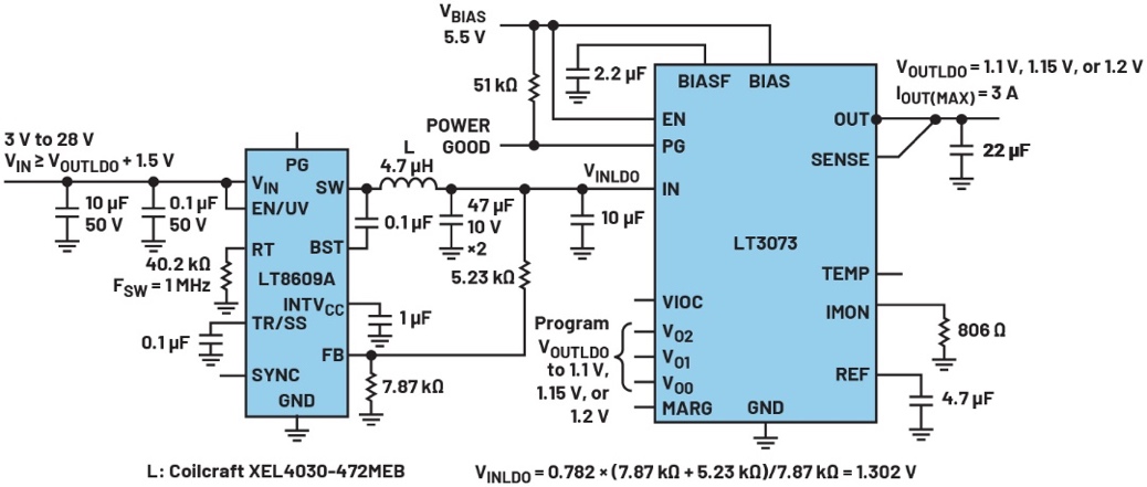
LDOs with VIOC provide an external signal via internal circuitry to control the output of the switching regulator powering the LDO, thereby maintaining a constant input-output voltage difference, as illustrated in Figure 1. Linear regulators are essentially transistor circuits capable of supplying power with relatively low noise, but they are highly sensitive to the input-output voltage difference, which also determines their efficiency. Switching regulators transfer energy through the rapid switching of power transistors (switches). Switching regulators utilise power switches, inductors, and diodes to efficiently convert the input voltage into a more suitable voltage for powering the LDO.
Figure 1. This VIOC system maintains a consistent input-output voltage difference for the LDO.
Using VIOC to Combine Buck Converters with LDOs for Enhanced Performance
A typical VIOC circuit employs a buck switching regulator to power an LDO with VIOC characteristics. The resulting circuit configuration is exceptionally robust, combining the high efficiency of a buck regulator with the low noise performance of an LDO. Buck regulators, also known as buck converters, are switching converters capable of efficiently converting an input voltage to a stable output below the input voltage.
The first step in creating a VIOC circuit is selecting the LDO and switching regulator. ADI offers multiple LDOs integrating VIOC functionality. The LT3045-1 and LT3041 series, along with the LT3073, LT3074, and LT3078 series, all feature the latest iteration of VIOC capability. The LT3045-1 and LT3041 linear regulators offer an output current range of 500 mA to 1 A and an input voltage range of approximately 2 V to 20 V, requiring only a single input supply. The LT3073, LT3074, and LT3078 offer output currents ranging from 3 A to 5 A with an input voltage range of 0.6 V to 5.5 V, requiring an additional low-current BIAS input supply. Any switching regulator with a feedback (FB) pin can be combined with these VIOC-enabled LDOs. However, note the following considerations before selecting a switching regulator for your design:
LDOs supporting VIOC can be used with any type of switching regulator topology, but are most commonly employed with buck regulators.
The LT3045-1 and LT3041 LDOs must be paired with switching regulators featuring a feedback (FB) voltage of 1 V or lower, enabling the LDO's VIOC pin to operate at 1 V (refer to the data sheet for details).
Within a VIOC system, switching regulators incorporating a compensation pin may exhibit greater stability compared to those without such a pin.
Switching regulator and LDO evaluation boards facilitate assessment of VIOC system hardware operation.
LDOs with VIOC functionality cannot be paired with Silent Switcher® 3 (SS3) switching regulators, as SS3 regulators lack a conventional FB pin.
Compared to typical VIOC circuits, μModule® regulators with integrated high-side feedback resistors cannot maintain a constant input-output voltage difference for the LDO.
Circuits employing VIOC require a dedicated voltage rail as the LDO's front end, rather than a front end supporting multiple voltage rails.
Compared to standalone LDO designs, VIOC necessitates additional components. The extra components required for a VIOC circuit include: an additional resistor in the feedback divider of the switching regulator powering the LDO, and an additional capacitor typically used at the switching regulator's output.
To simplify the design process, ADI provides guidance on which buck switching regulators are best suited for use with specific LDOs featuring VIOC characteristics. Table 1 lists suitable switching regulators recommended for combination with LDOs possessing VIOC, alongside descriptions for all LDOs. These pairings are based on the considerations outlined earlier; therefore, when constructing a VIOC circuit comprising a buck regulator and an LDO with VIOC characteristics, please follow the guidance provided above and in Table 1. Numerous VIOC circuit reference designs are available in the data sheets for the LDOs listed in Table 1.
Table 2 provides detailed specifications for the buck regulators listed in Table 1. This information assists designers in selecting regulators that not only meet electrical requirements but also comply with constraints such as the switch regulator's input voltage range, load current capability, and operating current. Beyond recommending switch regulators for VIOC, Table 2 also details the regulator's feedback pin voltage, available modes, evaluation board part numbers, and compensation pin availability.
Minimising Noise and High PSRR Advantages with VIOC
As described above, when an LDO is paired with a VIOC-capable and compatible switching regulator, it forms a system that perpetually maintains an optimal input-output voltage difference. This not only significantly reduces noise and achieves high PSRR but also enhances overall performance.
Table 1. Recommended LDO and Switching Regulators for VIOC Systems
LDO
LDO Specification
Recommended Switching Regulator 1
Recommended Switching Regulator 2
Recommended Switching Regulator 3
LT3041
20 V, 1 A, ultra-low noise, ultra-high PSRR linear regulator with VIOC control capability
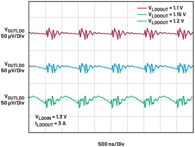
Some users merely wish to alter the LDO's output voltage without employing complex solutions to adjust the output voltage of the switching regulator supplying power to the LDO. In contrast to the circuit in Figure 1, the circuit shown in Figure 3 lacks a VIOC. Consequently, when the LDO output is increased or decreased, the output of the switching regulator remains unchanged. Figure 2 demonstrates that the PSRR performance of the circuit in Figure 3 deteriorates at higher LDO output voltages. This occurs because, when the LDO output voltage increases without a corresponding increase in the LDO input voltage, the ripple in the switching regulator's output voltage causes increased noise at the LDO output terminal.
Figure 2. These oscilloscope screenshots pertain to the circuit in Figure 3, demonstrating that noise caused by PSRR intensifies as the LDO output voltage increases.
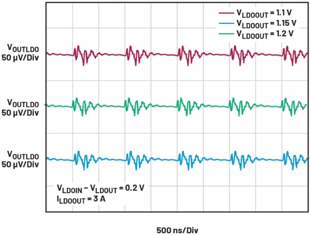
Now consider the advantages of VIOC over the examples shown in Figures 2 and 3. The VIOC system depicted in the circuit of Figure 1 maintains a consistent input-output voltage difference across the LDO when its output varies, thereby preserving a high level of PSRR designed to effectively suppress noise. The output voltage of the switching regulator automatically adjusts downward when the LDO output decreases and upward when the LDO output increases. Consequently, even when the LDO output voltage fluctuates across three distinct levels, the noise induced at the LDO output by the switching regulator's output voltage ripple remains at a low level, as illustrated in Figure 4.
Figure 3. This circuit does not utilise VIOC.
Advantages of VIOC: Enhanced Efficiency, Strengthened Protection and Optimised Operation
Beyond noise minimisation and high PSRR benefits, systems incorporating VIOC consistently maintain an optimal input-output voltage differential, ensuring efficient, secure and robust performance. The efficiency advantage is evident: when the LDO output voltage decreases while the input voltage remains constant (as illustrated in the circuit of Figure 3), the LDO's power dissipation increases and efficiency diminishes. For the VIOC system in Figure 1, even when the LDO output varies, VIOC maintains a constant input-output voltage difference, thereby keeping power dissipation unchanged.
Figure 4. These oscilloscope screenshots pertain to the circuit depicted in Figure 1, demonstrating that noise induced by PSRR remains consistently low. This is attributable to the circuit maintaining a constant input-output voltage difference across the LDO.
Furthermore, in systems without VIOC, certain conditions and faults may cause the LDO input-output voltage difference to increase to unacceptable levels. For instance, if both the switching regulator output and the LDO output are set to relatively high voltages, and an output short-circuit fault occurs on the LDO, the LDO input-output voltage difference may increase sharply. An output short-circuit fault on the LDO causes an excessively high input-output voltage difference across the LDO terminals, as there is no VIOC to force the switching regulator's output voltage down and maintain the set LDO input-output voltage difference. When the LDO output is shorted, the high input-output voltage difference during the fault significantly increases the LDO's power dissipation. This may cause the LDO temperature to exceed its recommended operating range, thereby compromising reliability.
Furthermore, the elevated input-output voltage difference during an LDO output short-circuit fault can prevent normal recovery after the fault is cleared. This occurs because many high-voltage LDOs incorporate a protective feature known as current-limiting foldback.
Current-limiting foldback is a protection technique employed in power supplies and regulators to reduce output current during overcurrent or short-circuit conditions. Unlike simple current limiting, which maintains a constant current during faults, foldback current limiting simultaneously reduces both output voltage and current, thereby lowering power dissipation in circuit components. This helps protect the power supply and connected devices from damage due to overheating and excessive current.
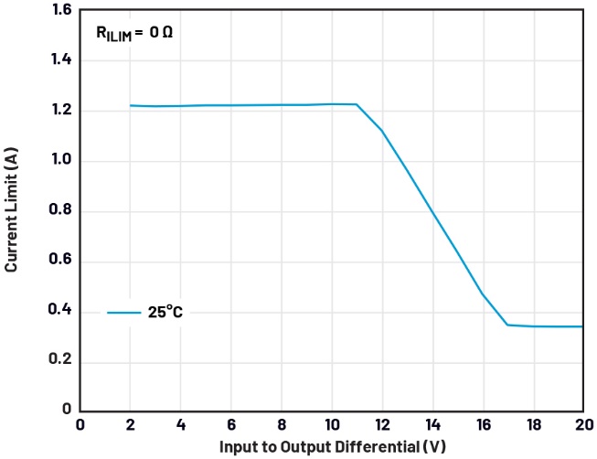
Figure 5 illustrates the typical foldback current limiting behaviour of the LT3041 LDO. Note that in Figure 5, the LDO is capable of delivering a lower current when the input-output voltage difference exceeds 11 V. Many ADI LDO data sheets include a section titled ‘Overload Recovery’, which explains why foldback current limiting prevents an LDO with a relatively high output voltage setpoint and load from returning to the correct output voltage once a short-circuit fault on the LDO output is cleared.
Figure 5. Typical current-limiting foldback of the LT3041 LDO
Current limiting foldback in circuits without VIOC will also prevent high-voltage circuits from starting up correctly. This occurs because when the circuit turns on, the LDO's output voltage initially starts at zero volts and gradually rises to the desired stable output voltage during normal operation. If the input voltage is relatively high during turn-on, the current limiting foldback may excessively restrict the LDO current, preventing the LDO output voltage from rising to the desired stable voltage. VIOC automatically maintains the correct switching regulator output voltage, thereby preserving the correct LDO input-output voltage difference and ensuring the circuit functions correctly under fault and start-up conditions.
Conclusion
Part One of this series laid the foundation for understanding how to design efficient, low-noise power systems using combinations of VIOC-enabled LDOs and buck regulators – the most common configuration in modern applications. It also examines recommended LDO-switching regulator pairings and their rationale, demonstrating how deliberate device selection significantly enhances system performance. This article illustrates how the VIOC feature reduces output noise, improves thermal efficiency, and strengthens system protection and performance during start-up and overload recovery.
Part Two of this series will explore how these devices maintain a constant input-output voltage difference and introduce practical tools to simplify VIOC system implementation.

 English