Abstract
As power supply designs increasingly prioritise smaller form factors, higher efficiency and improved thermal performance, noise issues are often deferred until the later stages of the design process, making them difficult to resolve effectively. Although the use of Silent Switcher® regulators or optimised PCB layout in the early design stages can help reduce noise, if these initial measures are not implemented in a timely manner, more fundamental circuit solutions such as buffer circuits can be employed to effectively mitigate noise problems.
This article begins by examining issues related to switching ringing, using a synchronous buck regulator as an example. It then explains how to design and optimise buffer circuits to suppress this ringing. We will utilise LTspice® and typical parasitic models to simulate the ringing phenomenon on a standard PCB, and demonstrate the impact of calculated buffer circuit values on both ringing and overall efficiency.
Background information
Modern DC-DC converters are constantly evolving towards higher efficiency and smaller form factors. To achieve this, a common approach is to increase the switching frequency. Whilst this allows for the use of smaller inductors and capacitors in the design, the effects of parasitic effects—that is, the unintended inductance and capacitance generated by components and PCB traces—become more pronounced. At higher switching speeds, the interaction between the circuit and these parasitic effects can lead to severe voltage overshoot and ringing at the switch (SW) node.
Such ringing not only subjects the FET to additional voltage stress but also generates unwanted electromagnetic interference (EMI). EMI is an electromagnetic signal that disrupts system operation through electromagnetic induction, electrostatic coupling or conduction. In industries such as automotive, medical, and test and measurement, EMI represents a critical design challenge. Only by strictly complying with EMI standards can products be guaranteed to pass certification and reach the market on schedule.
Understanding the parasitic effect
Voltage overshoot and ringing at the switching nodes of a buck converter are a direct result of the interaction between high switching speeds and the parasitic inductance and capacitance within the circuit. These parasitic effects are caused by the PCB traces and the components themselves, particularly the FETs.
Essentially, the stray inductance of the PCB traces and the FET package forms an LC resonant circuit with the FET’s parasitic output capacitance (COSS). Consequently, the layout and selection of the MOSFET are critical design factors.
The magnitude of stray inductance varies depending on the design; however, for our example simulation, assuming a stray inductance of 5 nH around the power-stage FET is a reasonable starting point. This value may increase significantly if the layout is poor, as stray inductance can increase by up to 10 nH for every 25 mm (1 inch) of trace length.
Figure 1 shows a typical power controller circuit using the LTC3854, where the red sections indicate the expected parasitic effects.
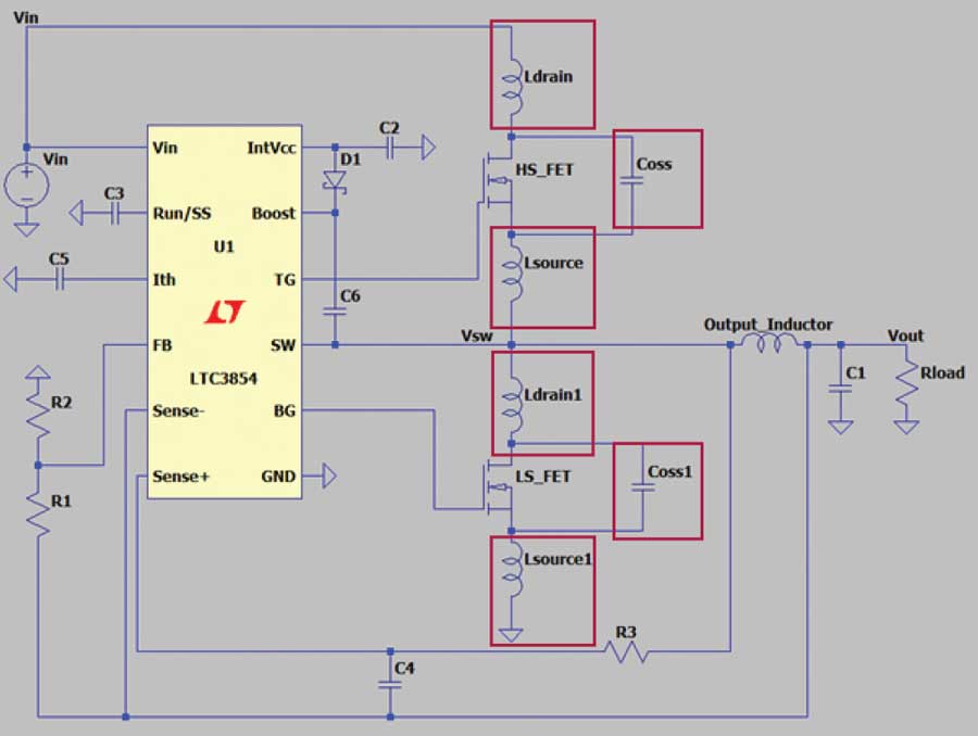
Figure 1. Power supply circuit incorporating circuit parasitic effects
Buffer Circuit Design: Theory and Calculations
Definition and Operating Principles of Buffer Circuits
Having understood the noise generated by switching operations and the parasitic parameters involved, we can now introduce methods for suppressing this unwanted energy. A buffer circuit typically consists of a series resistor-capacitor (RC) network, which can be used to absorb voltage spikes and ringing that occur at the switching node.
The function of the buffer circuit is to provide a controlled dissipation path for the high-frequency energy generated by the parasitic LC resonant circuit. When the switch turns off, the buffer capacitor begins to charge, absorbing the energy that would otherwise cause ringing. The buffer resistor subsequently dissipates this stored energy as heat, thereby effectively suppressing oscillations. By introducing a new resonant frequency and adding resistance to the circuit, the buffer circuit reduces the peak voltage and duration of the ringing, thus protecting the power switch from overvoltage stress.
Figure 2 illustrates a typical buck converter, with the buffer circuit located between the switch node and ground, as close as possible to the MOSFET.
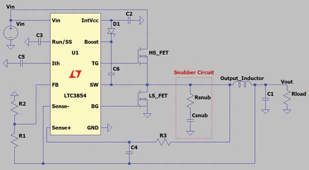
Figure 2. The location of the buffer circuit in a typical power supply design
Steps for calculating a buffer circuit
1. As outlined in the measurement techniques section, first measure the ringing frequency at the switch node (i.e. the peak-to-peak distance between the first and second peaks). Note: Whilst the discussion in this article relates to simulation, for actual PCB measurements, the bandwidth limit function must be disabled and the oscilloscope’s ground lead must be shorted to ensure the ringing is visible. The required measurement techniques will be briefly outlined later in this article for the reader’s reference.
2. Add a capacitor between SW and GND to reduce the ringing frequency (fr) to approximately half of the measured value. In this step, it is recommended to try different capacitance values.
3. Divide the added capacitance value by 3 to obtain the parasitic capacitance (CP).
4. Once the parasitic capacitance is known, the parasitic inductance (LP) can be calculated as follows:

The characteristic impedance is calculated as follows:

To reduce ringing, a buffer resistor is required, with an impedance roughly equal to that calculated in Equation 2, typically amounting to a few ohms.

Next, select the capacitance value: multiply the CP value calculated using Equation 3 by a coefficient between 1 and 4.
Simulation and analysis using LTspice
Having established a basic understanding of noise generation, measurement and the calculation of initial buffer circuit values, the next step is to simulate these effects. This section uses LTspice to demonstrate the impact of PCB parasitic effects on switching node ringing and overshoot, as well as the effectiveness of buffer circuits.
We will conduct the following analysis to compare the operating behaviour of a buck converter with and without a buffer circuit.
1. Modelling parasitic effects: First, we will construct a model incorporating parasitic parameters to demonstrate the ringing and overshoot occurring at the switching node in the absence of any buffer circuit.
2. Impact of the initial buffer circuit: We will then simulate the circuit using the preliminarily calculated buffer circuit values to demonstrate the ringing attenuation effect.
3. Optimisation of the buffer circuit: We will then iteratively adjust the values of the buffer circuit components to find the balance between effective ringing suppression and minimised power loss.

Figure 3. Comparison of the advantages and disadvantages of measurement techniques
4. Efficiency analysis: Finally, the overall efficiency of the step-down converter is compared in scenarios with and without the optimised buffer circuit, in order to quantify the impact of the buffer circuit.
Modelling of parasitic effects and ringing measurements
The LTC3854 synchronous buck controller is a good example of how poor layout can introduce significant parasitic effects, leading to ringing at the switching nodes. As this device uses external FETs, the impact of layout is particularly pronounced. For this simulation, we have modelled the effects of poor layout by introducing 5 nH of parasitic inductance. This is a reasonable value, as every 25 mm of PCB trace can introduce 10 nH or more of parasitic inductance.
Before calculating the values for the buffer circuit, it is essential to understand the severity of this issue. This is typically done by monitoring the switching nodes with an oscilloscope. To accurately capture the rising voltage waveform, the oscilloscope’s voltage per division should be set appropriately to cover the full voltage range (0 V to VIN), and the time base adjusted to view individual transitions.
The use of appropriate probing techniques is key to obtaining accurate measurement results. A common error is the use of long ground leads on the oscilloscope probe, which introduce parasitic inductance themselves. This inductance may cause artificial ringing in the measurement, thereby providing a misleading representation of the actual switching activity. To significantly reduce loop inductance and improve measurement fidelity, long leads must be replaced with short ground springs.
This article focuses primarily on theory and simulation; a detailed explanation of correct hardware measurement techniques falls outside its scope, though this is a highly important topic worthy of dedicated discussion. The images in Figure 3 demonstrate the significant differences in measurement results, indicating that longer ground leads may introduce severe overshoot and ringing, leading to incorrect assessments of circuit performance.
Simulation results for the circuit without a buffer

Figure 4. Schematic diagram illustrating the parasitic effects of printed circuit boards and components

Figure 5. Observed switching nodes and associated overshoot and ringing
Figure 4 shows the various parasitic inductances and capacitances modelled in the buck converter circuit. Figure 5 illustrates the effect of these parasitic parameters on the waveform at the switch (SW) node. The LC resonant circuit formed by these components can cause severe overshoot and ringing.
Simulation results show that the voltage peaks exceed 18 V, which is significantly higher than the expected 12 V. This overshoot poses a major risk, as its amplitude may exceed the MOSFET’s absolute maximum rated voltage, potentially damaging the device or compromising its long-term reliability. Ringing is also a concern, as it indicates that the MOSFET is not operating in its clearly defined on/off states.
Figure 6 shows that the overall efficiency of this circuit is 96.3%, which at first glance appears to be high. However, it should be noted that this efficiency was achieved without a buffer circuit. The following section will demonstrate that the addition of a buffer circuit—which is essential for suppressing ringing—has a minor yet quantifiable impact on efficiency.
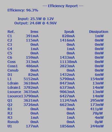
Figure 6. Efficiency of the original circuit
Parasitic models and uncalculated buffer circuits
Figure 7 shows the same schematic as Figure 4, but with a simple RC buffer circuit added between the switch node and ground. Please note that the values for the buffer circuit are merely initial estimates and have not yet been calculated, so they are not optimal.
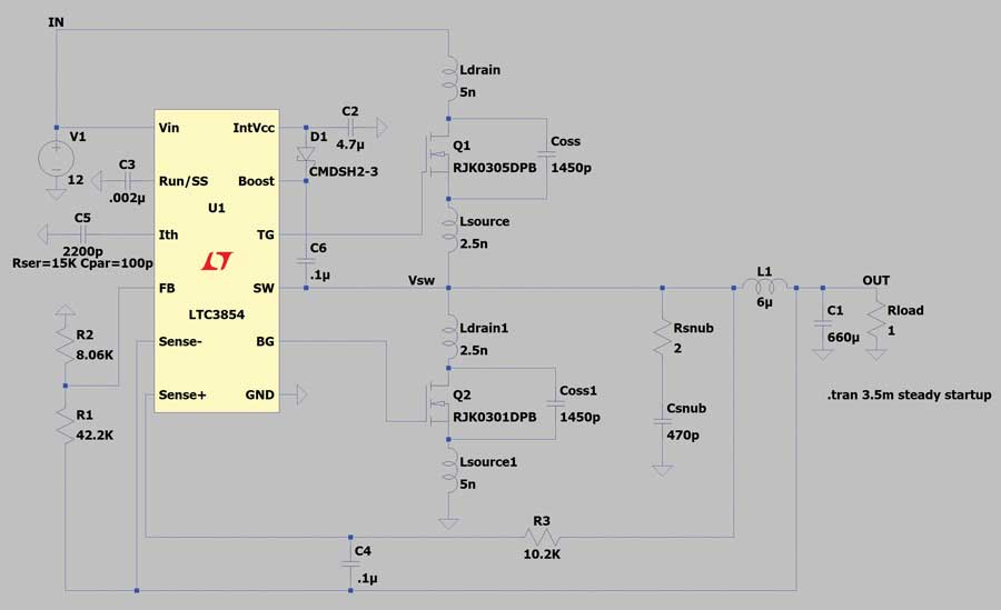
Figure 7. Schematic diagram showing the buffer circuit
As shown in Figure 8, the waveforms at the switching nodes have improved significantly. The peak overshoot voltage has dropped to 14 V, a reduction of 4 V, and the oscillations occurring after turn-on have been significantly reduced. However, efficiency has fallen sharply to 58.9% (see Figure 9), with most of the losses attributable to the buffer resistors. This indicates that, whilst an unoptimised buffer circuit can mitigate ringing, it also leads to a significant reduction in efficiency.
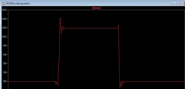
Figure 8. Ringing at the switch node following the introduction of a buffer circuit
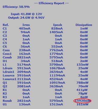
Figure 9. Efficiency when using the initial buffer circuit values
Optimisation of buffer circuits
We will now optimise the values of the buffer circuit using the calculation method described earlier in this article. The aim is to select an RC buffer circuit that effectively suppresses ringing without causing excessive power loss.
First, determine the circuit’s parasitic LC components. Initial simulation (without the buffer circuit) shows a ringing frequency of 23.41 MHz.
Next, add a known capacitance between the switch node and ground to observe the change in ringing frequency. After applying a 14,000 pF capacitor at the switch node, the new simulation results show that the ringing frequency has dropped to 12 MHz. The parasitic capacitance can be determined using the resonance frequency formula fo = 1/(2 × π√LC). The change in frequency is caused by an increase in total capacitance. The new total capacitance (Ctotal) is:
Ctotal = Cparasitic + Cadded
The relationship between the original frequency (fold) and the new frequency (fnew) is:

Solve Cparasitic:
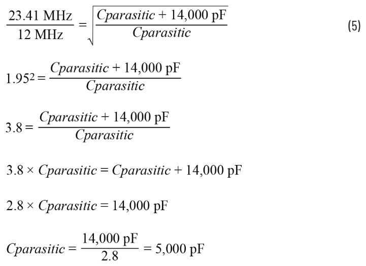
This indicates that the circuit has a parasitic capacitance of approximately 5,000 pF. The parasitic inductance can be calculated using the parasitic capacitance:
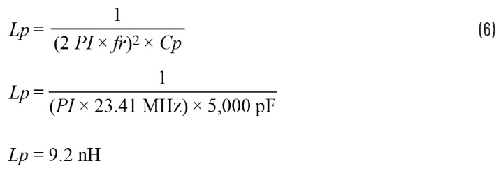
The impedance of this circuit is calculated as follows:
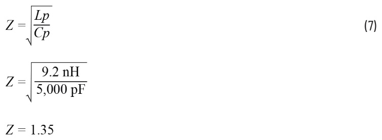
The buffer resistance is set to a value greater than the characteristic impedance mentioned above; in this example, the standard value is 1.5 Ω.
Next, the value of the buffer capacitor Csnubber should typically be at least equal to the parasitic capacitance, and may be up to four times that value. For this initial simulation, a value twice that of the parasitic capacitance is used to ensure sufficient energy dissipation; thus, Csnubber is set to 2 × Cparasitic = 2 × 5,000 pF = 10,000 pF.
Once the buffer resistor and capacitor have been optimised, these values are substituted into the LTspice simulation to observe the circuit’s behaviour.
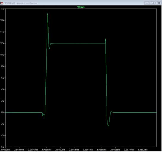
Figure 10. Switching node ringing when using a buffer circuit with values of 1.5 Ω and 10,000 pF
Figure 10 shows the waveform obtained using a 1.5 Ω + 10,000 pF buffer network. As expected from the optimised design, the ringing has been significantly reduced. With these calculated buffer circuit values, the overshoot voltage has also been reduced from over 18 V to 17.2 V. Although some overshoot remains, this result highlights the inherent trade-off in buffer circuit design: the buffer circuit values required to completely eliminate overshoot and ringing typically result in increased power dissipation and reduced efficiency.
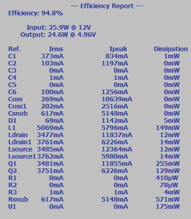
Furthermore, the overall efficiency is now 94.8% (see Figure 11), representing a very significant improvement compared to the 58.9% achieved when using a buffer circuit without calculated values. The use of a buffer circuit inevitably has some impact on efficiency, as the resistors consume a small amount of power. However, this impact on efficiency can be minimised by optimising the component values based on the parasitic LC resonant circuit.
Conclusion
Understanding and suppressing switching node ringing is a crucial step in designing a reliable switching regulator. As discussed in this article, this high-frequency noise is not an inherent flaw, but rather a direct result of a parasitic LC resonant circuit formed by the inductance of the PCB traces and the capacitance of the switching components.
By employing a systematic analytical approach to accurately simulate the unmitigated ringing frequencies and associated voltage overshoots, this problem can be readily resolved. This method enables the calculation of precise values for the buffer network, where the resistors match the parasitic impedance to bring the circuit to a state of critical damping, whilst the capacitors act as energy sinks.
Simulation examples clearly demonstrate that a carefully designed buffer circuit is a simple yet effective solution. It offers a significant improvement in EMI performance and system reliability at the cost of minimal and controllable power dissipation. In summary, by incorporating this simple yet powerful RC network, a noisy and susceptible power supply can be rapidly transformed into a low-noise, stable and reliable power supply, ensuring that the final product is durable and compliant with standards.

 English