Abstract
Ultra-thin, low-noise, multi-phase power supply solutions are continually pushing the boundaries of traditional high-density electronic systems. Combining compact dimensions with high current capability, these solutions enable designers to meet stringent transient and efficiency requirements without sacrificing valuable PCB space. Advanced multi-phase architectures support fast transient response, lower output ripple and improved thermal performance, which is particularly beneficial for applications with thermal constraints and where signal integrity is critical.
This article presents a practical solution implemented using ultra-thin, low-noise μModule regulators. By utilising multi-phase interleaving and parallel operation, this solution achieves extremely low output noise and electromagnetic interference (EMI) within a compact form factor, whilst increasing the output current to 16A. This approach is particularly well-suited to sensitive analogue circuits, high-speed data interfaces and densely populated PCBs in data centre, 5G telecommunications and industrial automation applications.
Introduction
Modern electronic systems, such as cloud servers, telecommunications infrastructure and advanced industrial automation equipment, typically require higher performance within increasingly constrained spaces. Faced with rising load current demands and ever-shrinking circuit board areas, designers must deliver robust, high-current solutions without compromising efficiency, noise performance or signal integrity. At the same time, the widespread use of sensitive analogue circuits and high-speed data interfaces makes low noise and minimised electromagnetic interference (EMI) increasingly critical.
The LTM4732 addresses these challenges by utilising an ultra-thin, high-current multi-phase architecture and ADI’s groundbreaking Silent Switcher 3 (SS3) technology. Measuring just 6.25 mm × 4 mm × 1.92 mm, this μModule regulator is ideally suited to space-constrained applications with strict height limitations, where every millimetre counts. Its overall height is virtually equivalent to that of a surface-mount 1206-package capacitor, allowing it to be mounted on the underside of the PCB, thereby freeing up space on the front of the board. By integrating SS3 technology, this device achieves excellent noise performance, with low-frequency output noise as low as 4 μV rms, and significantly reduced conducted and radiated EMI. Traditional low-dropout (LDO) regulators often sacrifice efficiency for low-noise performance and may require an additional regulation stage following the switching converter. In contrast, the LTM4732 achieves both high efficiency and ultra-low noise characteristics within a single, compact module. Consequently, the power supply system requires no additional LDO stage, simplifying the design whilst still meeting the stringent noise requirements of sensitive analogue and high-speed digital systems. The high conversion efficiency further reduces power loss and heat generation, making this solution ideal for applications where thermal performance and energy efficiency are paramount.
Multiphase Operation and Interleaving in Power Modules
Modern high-current power modules (such as the LTM4732) utilise multiphase operation to achieve outstanding efficiency, noise and transient response performance. In a multiphase topology, several converters operate in parallel, with each phase switching at the same frequency but maintaining a fixed phase shift relative to the other phases. The interleaving of switching events is a key advantage of this architecture.
Phase Staggering and Ripple Reduction
When N phases are staggered, the time offset for each phase is:

For example, in a four-phase system, each phase is offset by 90°. This interleaving ensures that switching events are evenly distributed across the switching cycle, thereby effectively increasing the output ripple frequency:

Here, N represents the number of phases, and fsw is the switching frequency per phase.
The higher effective ripple frequency, combined with the partial cancellation of the phase currents at the output node, results in a significant reduction in output voltage ripple. For an ideal multi-phase system, the peak-to-peak ripple voltage is roughly inversely proportional to the number of phases. Consequently, designers are able to achieve stringent ripple targets using smaller output capacitors, thereby reducing board area and the number of components.
Output Capacitance and Transient Response
During rapid load transients, the initial output voltage deviation depends primarily on how quickly the circuit can deliver current to the output capacitance before the control loop responds. In interleaved multiphase converters, phase interleaving increases the effective ripple frequency at the output, shifting the ripple energy to higher frequencies whilst shortening the intervals during which the load receives current.
Consequently, transient load demands are distributed across multiple phases, thereby reducing the instantaneous voltage deviation per ampere of load step. Measurements show that during large load transitions, the circuit is able to recover stably and keep the voltage deviation within a reasonable range, even at high output current levels.
Current Scaling and Thermal Management
Another advantage of multiphase operation is that current scaling is very straightforward. The total output current capability increases linearly with the number of phases:

Connecting multiple modules in parallel increases the total current output whilst distributing thermal and electrical stresses across the phases, thereby enhancing reliability and simplifying thermal management.
Staggering the phases of multiple converters reduces output ripple and distributes heat evenly across the phases, thereby improving current capacity and efficiency. Consequently, multi-phase architectures are particularly valuable in high-performance applications where noise and thermal management are critical considerations.
Design Considerations and Guidelines for the LTM4732 in Multi-Phase Architectures
Overview
When using the LTM4732 in multi-phase applications, particular attention must be paid to configuration, synchronisation and layout to ensure optimal performance and reliable current sharing. This section summarises practical guidelines and best practices for high-current applications, including how to connect multiple modules in parallel, effectively reduce noise and manage thermal performance.
Parallel Configuration
To support higher load currents via a single output, two or more modules can be configured in parallel, i.e. by connecting the VIN, VOUT, VOSNS and COMP pins of all devices together. This configuration ensures that all phases share voltage sensing and compensation, which is critical for accurate current sharing and stable operation. Figure 1 illustrates a four-phase configuration in which all modules are connected in parallel.

Figure 1: Four-phase LTM4732 buck converter configuration with modules in an interleaved parallel arrangement
Clock synchronisation and phase locking
Multiple LTM4732 converters can be configured to support multi-phase operation, achieved by synchronising the clocks of the slave and master phases. To ensure reliable synchronisation, the frequency of the master phase’s free-running oscillator should be set to at least 20% higher than that of the slave phase prior to synchronisation, and the master phase’s CLKOUT should be applied to the slave phase’s SYNC pin.
The PHMODE pin sets the relative phase shift between the converters. When PHMODE is grounded, the phase shift is 180°; when PHMODE is left floating, the phase shift is 120°; and when PHMODE is connected to INTVCC or an external power supply greater than 3 V, the phase shift is 90°. For three-phase operation, PHMODE is left floating to achieve a 120° phase shift, whilst for four-phase operation, PHMODE is connected to INTVCC to achieve a 90° phase shift, as shown in Figures 2a and 2b respectively.
This configuration ensures deterministic phase interleaving, thereby reducing output ripple and improving EMI performance.
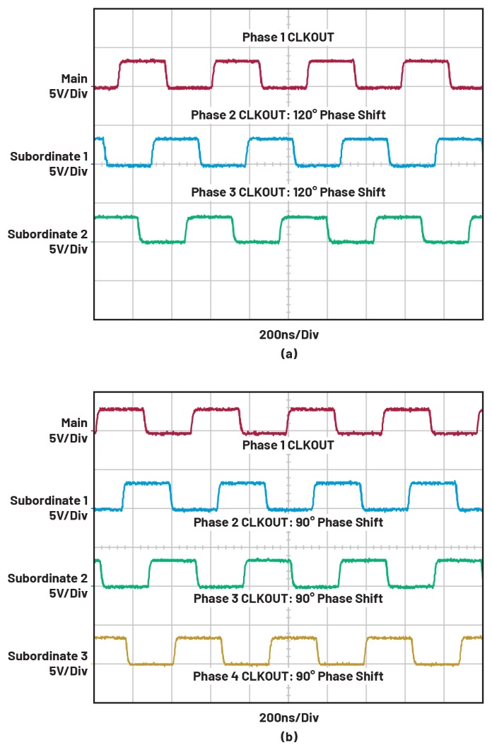
Figure 2: Waveforms illustrating 120° and 90° phase shifts between phases: (a) three-phase configuration; (b) four-phase configuration
Measurement Results and Performance Verification
Efficiency, Power Loss and Thermal Performance
Figure 3 compares the efficiency of single-phase and four-phase configurations under different load currents. At a 4 A load, the efficiency of the four-phase configuration is 83 per cent, which is superior to the 75.5 per cent achieved by the single-phase configuration. This improvement in efficiency is due to the fact that, when the load is shared across multiple phases, the RMS current per phase is reduced and conduction losses are lowered.
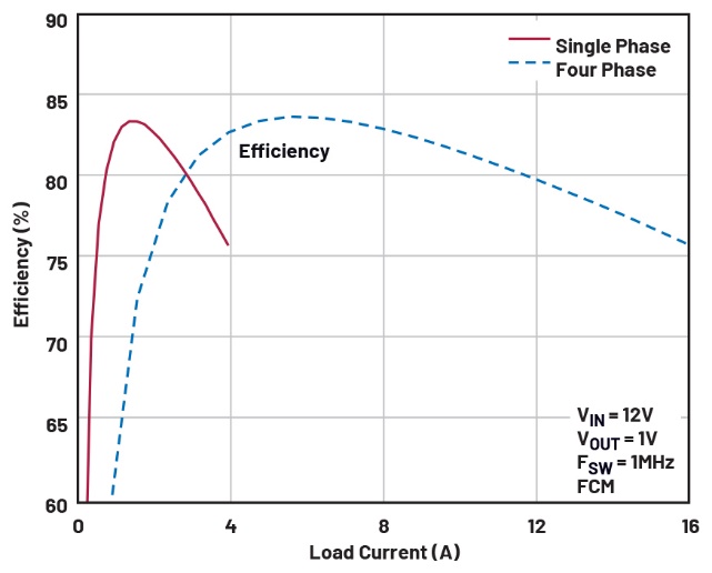
Figure 3: Efficiency Comparison between Single-Phase and Four-Phase LTM4732 Configurations
We evaluated the efficiency, power dissipation and thermal behaviour of the four-phase configuration under steady-state load conditions to characterise its system-level performance at high output currents.
Across the entire load range, measured efficiency remained at a high level, whilst total power dissipation increased gradually with rising output current, as expected. The load current is shared across four interleaved phases, reducing the current stress on each phase. This helps to minimise conduction losses within each module and enables the system to operate stably at higher load levels.
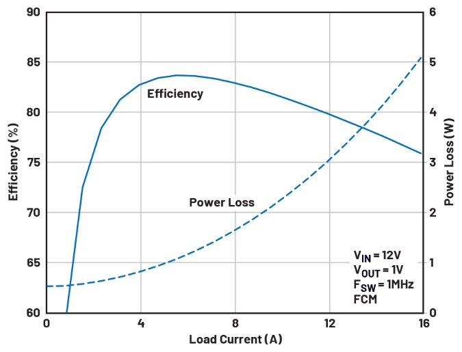
Figure 4: Efficiency and power loss of the four-phase interleaved LTM4732 at 1 MHz fSW, 12 VIN and 1 VOUT
The thermal image shows that the temperature distribution across the four modules is uniform, with no localised hotspots observed during operation. The peak temperature of the device is well controlled, demonstrating that current sharing and thermal diffusion are highly effective in a multi-phase configuration. These balanced thermal characteristics help to enhance current output capability and improve system reliability in thermally constrained applications.
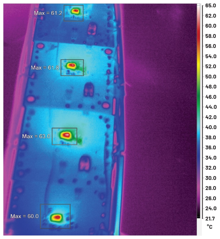
Figure 5: Thermal image of the four-phase interleaved LTM4732 demonstration board at 1 MHz fSW, 12 VIN and 1 VOUT
In summary, the measured efficiency, power consumption and thermal results confirm that the four-phase LTM4732 solution offers robust high-current performance, controllable losses and uniform thermal stress distribution.
Transient Response
Figure 6 shows the output voltage response of the four-phase configuration to load steps ranging from 8A to 16A. During high-load switching, the converter maintained a controlled voltage deviation and stable recovery behaviour. The output settled rapidly without sustained oscillation, indicating that the loop possesses sufficient stability and that current sharing across the phases is effective. Measurements of voltage deviation, normalised by the applied load step, indicate that the multi-phase architecture not only offers efficient current transfer capability but also exhibits a low effective output impedance. As the current is shared across the phases, transient voltage drops are effectively suppressed, enabling the system to achieve rapid transient recovery even under highly dynamic load conditions.
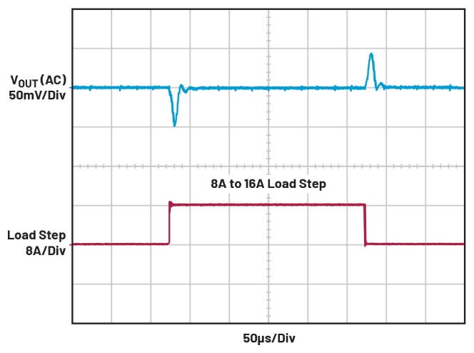
Figure 6: Load step transient waveform for four-phase operation
Bode plot (frequency response)
Figure 7 shows the control loop gain and phase response measured for the four-phase configuration under nominal operating conditions. The loop exhibits a distinct single crossover frequency and sufficient phase margin, indicating that the system is capable of stable operation across the entire frequency range. The measured crossover frequency is approximately 66 kHz, with a phase margin of 53°, achieving a balance between transient response and stability. No low-frequency instability or excessive peaking was observed, and the loop gain declines smoothly beyond the crossover point, consistent with the expected current-mode control behaviour.

Figure 7: Bode plot of the four-phase LTM4732
Troubleshooting and Recommendations
Conclusion
The LTM4732 sets a new performance benchmark for high-current, low-noise power delivery in space-constrained applications. With its ultra-thin package, advanced multi-phase interleaved design and SS3 technology, the LTM4732 delivers outstanding efficiency, extremely low output noise and robust EMI performance. Test results confirm that parallel operation of multiple modules increases output current, reduces ripple and optimises thermal management, eliminating the need for a downstream LDO regulator in many designs.
By adhering to the design considerations and best practices outlined in this article, engineers can confidently employ the LTM4732 in demanding systems to optimise both performance and reliability. As power density and noise requirements continue to rise, multi-phase solutions such as this offer a flexible and future-proof approach to next-generation electronic design.

 English