Abstract
For any product design requiring high-speed clocks, electromagnetic compatibility (EMC) compliance can be a major challenge. This article provides an overview of printed circuit board (PCB) design from the perspective of electromagnetic (EM) field orientation, with the aim of helping readers pass electromagnetic interference (EMI) compliance testing on the first attempt. The techniques used to reduce EMI will also mitigate interference, reflecting general PCB layout principles. This article is divided into three sections. The first section introduces fundamental physics concepts to help readers understand why the techniques described here can mitigate EMI in PCB layout. Section 2 provides examples illustrating how the material from Section 1 can be applied to actual PCB layouts. Finally, Section 3 discusses PCB layout strategies for complex circuit boards that meet the requirements of the proposed solutions.
Introduction
Why is compliance often the last consideration in the design process? This is usually because the entire system must be made operational before any actual testing can begin. If issues are discovered late in the design process, it may be necessary to modify the printed circuit board (PCB), and this work is always costly when multiple people are involved late in the product design cycle. This situation is often regrettable. In reality, however, simply following the best practices described in this article will ensure compliance with electromagnetic compatibility (EMC) requirements (radiation, conduction, or susceptibility). The methods outlined here help integrate electromagnetic interference (EMI) compliance throughout the entire PCB architecture, design, and layout process. The purpose of this article is not merely to demonstrate how to design a PCB to pass EMC testing, but rather to help readers understand the underlying principles and mechanisms so that they can apply these principles in other contexts.
The fundamental principles behind EMI, interference, and susceptibility are very simple. The key to reducing EMI lies in controlling and confining electric and magnetic fields. Simply put, if an electromagnetic (EM) field is exposed to free space and can expand further, interference and EMI will result. How can this field confinement be achieved? Simply by designing the PCB (and any connected cables) so that there is zero net accelerating charge throughout. This means that for every charge being accelerated, there is another charge nearby that is accelerated in the opposite direction. When these events occur simultaneously in the far field, the effects of each charge will cancel each other out. Without field energy, no EMI or interference is generated. In other words, all electromagnetic field energy will be confined within the components or within the PCB dielectric between the signal traces and the ground plane. The above concept applies to traces on a circuit board, but in reality, long antennas with unconstrained fields in isolated systems pose a greater problem. We will discuss this topic in a future article.
Physical Principles of Static and Dynamic Forces on Charges
Charges move only when exposed to an electric field. The electric field at a given point in space can be static (such as the field produced by a stationary charge). The electric field at a given point can also vary with time (such as the field produced by a moving charge). When a charge begins to move, a magnetic field is generated. Similar to electric fields, magnetic fields can be either static or time-varying. According to the Lorentz force equation F = q (E + vxB), we know that a moving charge in a magnetic field experiences a force whose direction is either toward or away from the moving charges generating the magnetic field. Since only an electric field can exert a force on a charge, the magnetic field is actually an electric field generated by relativistic effects. This is a manifestation of the original Coulomb field of a moving charge. Electric and magnetic fields are essentially the same physical phenomenon, merely manifesting in different forms under different reference frames.
When these fields vary with time, they may generate radiation or EMI. Charges can be stationary, moving through space, or accelerated. Radiation is produced only when charges are accelerated. This is essentially a simple fact: a magnetic field is, in essence, an electric field, and accelerated charges cause this relativistic field to release its energy. Accelerated charges satisfy both Ampère’s law and Faraday’s law, thereby generating a propagating electromagnetic field in space. By carefully examining the Maxwell equations shown below, we can mathematically explain this phenomenon. Among them, the third and fourth equations, proposed by Ampère and Faraday, are key to understanding radiation and EMI.
Gauss's Law for Electric Fields:

Gauss's Law for Magnetic Fields:

Ampère–Maxwell's Law:

Faraday's Law:

These equations show that there are other ways to generate electric and magnetic fields besides using electric charges. Changing or dynamic fields can also create fields, which in turn propagate electromagnetic energy through free space or on a PCB. The Poincaré energy vector describes the motion of this energy.
Poincaré vector:

Wherever there is voltage and current, a field always exists. Electromagnetic fields are carriers of information and energy. Eliminating electromagnetic fields is neither feasible nor desirable. Our goal is to control the location of the fields so that they do not exert forces on disturbed charges (i.e., to avoid interference) and do not radiate into free space (i.e., to avoid EMI).
The good news is that, with proper PCB design, these fields can be automatically constrained.
Whether the charges are moving or stationary, any charge distribution will self-organize to minimize the energy stored or dissipated due to that distribution.
This principle applies not only to electrostatic energy but also to magnetic energy. The charges involved in the distribution will first self-organize to minimize the stored energy. Over time, this arrangement will settle into a state that dissipates as little energy as possible. This behavior is, in fact, the result of the forces of interaction between the charges.
So, how should a circuit board be designed to minimize the energy it stores? This can be achieved by placing a ground plane near signal and power paths. The proximity of the ground plane allows the copper geometry to store the least amount of electrical and magnetic energy. This is because the electric field will draw charge from the ground plane, thereby nearly canceling out the net electric field observed from the outside, as seen from the exterior of the dipole. Similarly, when charges accelerate, Faraday’s law induces a current in the ground plane, thereby counteracting the external magnetic field. When designing a PCB, care must be taken to ensure that this natural phenomenon can occur unimpeded. It is important to note that both of these effects occur almost instantaneously; the only delay is the speed at which the signal propagates from the charges to the ground plane (i.e., the speed of light, C).
The preceding section also described the properties of transmission lines. Most engineers are thoroughly familiar with transmission lines and use them daily in high-speed circuits. To avoid interference and EMI, these transmission line techniques must be incorporated into all PCB applications. Microstrip transmission lines are perhaps the most commonly used structure in PCB design; they are essentially just a trace above the ground plane. Theoretically, this confines the electric and magnetic fields to the space between the trace and the ground plane. As shown in Figure 1, within volume A, Maxwell’s equations indicate that the total enclosed charge equals the integral of the electric flux through the surface of that volume. Since zero charge is enclosed, and the separation of equal and opposite charges occurs within the same location, the net electric field outside the surface will approach zero. The transmission line, surface B, will enclose zero accelerated charge. Maxwell’s equations show that if the net current through surface B is zero, then the line integral of the magnetic field around that surface will also approach zero. According to Faraday’s law, the line integral around surface C will likewise approach zero.
It is important to note that the space between the transmission line and the ground plane cannot be zero (otherwise, the external field would be zero). In RF and high-speed digital applications, 50 Ω transmission lines are typically used to maximize signal bandwidth. For power circuits, however, designs with much lower impedance—typically only a few ohms—are used.
It is worth noting that all this physical knowledge can be summarized into three best practices, which should be followed during the layout process. The next section will introduce each of these practices in turn.
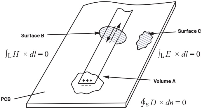
Figure 1. Schematic diagram of the electric and magnetic fields around a transmission line.
Best Practices
#1 Aim for zero net accelerating charge.
This practice encourages designers to pay close attention to current paths in PCB design. Based on Faraday’s law, consider whether the board layout allows for the natural generation of counteracting currents. Keep in mind that the presence of any current implies that it has undergone a change at some point to reach its current value.
#2 When designing the layout, confine electric and electromagnetic fields to specific, smaller areas.
This is the result of the first practical application. If the layout design can achieve zero net accelerated charge, the electric field will also be effectively confined to a specific area. During the layout process, designers need to pay special attention to this point, because both electric and magnetic fields are necessary for energy transfer.
#3 Focus on electromagnetic fields, not just voltage and current.
Energy and information are transmitted via electromagnetic fields, not through the copper traces on the PCB. If a microstrip line has defects, it is impossible to completely eliminate external electromagnetic fields. The higher the transmission line impedance, the less constrained the fields are. Fortunately, lines with higher impedance (50 Ω at maximum bandwidth) typically operate at lower currents, with their initial values limited to the voltage divided by the 50 Ω characteristic impedance. Power planes have lower impedance (which is ideal) but operate at higher currents (which is less desirable) and must be underdamped (i.e., have minimal effective resistance); otherwise, losses would be too high. These high-Q circuits generate significant radiation, an issue that will be discussed in detail in subsequent articles. From an EMI perspective, natural phenomena actually assist designers rather than creating obstacles—charges always arrange themselves in a way that minimizes energy consumption (whether stored or dissipated).
PCB layout can cause EMI and interference due to magnetic coupling or electrostatic coupling (mutual inductance and mutual capacitance). This coupling occurs primarily because the structures on a PCB used to transmit energy and information are not perfect; they cannot fully confine electromagnetic fields the way a coaxial cable does. The space (dielectric) between waveguides (traces and ground planes) will lead to interference and EMI unless the geometry can completely confine the field.
The next article will delve into practical PCB layout, identify radiation sources resulting from inadequate layout techniques, and propose improvement methods. We will analyze the following common scenarios in PCB layout.
On a PCB, field confinement is typically lost when the following situations occur:
- Signal Transfer Between Layers
- Signals share the same space above the common ground plane
- Signals cross each other above the common ground plane
- Signals Running in Parallel
- Appearing at the edge of the scene
- Signals propagate along microstrip lines or other defective transmission lines
Conclusion
This paper presents the fundamental physical knowledge and thought processes required for designing PCB layouts for low-radiation and EMI compliance testing. Through analysis, we have learned that only electric fields can act on charges, and that the magnetic field generated by moving charges is, in fact, a relativistic electric field. When charges are accelerated, Maxwell’s equations and the Poynting vector reveal how fields propagate in free space. All PCB copper geometries can be regarded as transmission lines capable of utilizing the field’s influence on charges to confine them within specific areas of the PCB. Building on this foundation, Part 2 of this article explains how to layout a PCB to minimize unconstrained fields as much as possible. These unconstrained fields are the primary sources of interference and EMI. Unconstrained fields can originate from two sources: the circuit itself or external factors (sensitivity). The next article will discuss these two sources separately.
Simply follow these three best practices to address both the key points and all physical effects.
Whether the charge is in motion or at rest, any charge distribution will naturally arrange itself in such a way as to minimize the energy stored or dissipated as a result of that distribution.

 English










