What is the AI chip used for? Data reasoning, machine learning, and deep learning, we have more and more access to these AI knowledge, because more and more companies have entered the development of AI chips. Which AI chips have entered the public already? This article will take you to understand it well.
Short Brief
The emergence of today's AI development is mainly due to the tremendous progress in machine learning, especially the deep learning in machine, and it exerts great power with the support of big data and big computing power.
The three key basic elements of AI are data, algorithms, and computing power. With the widespread application of cloud computing, especially deep learning has become the mainstream method of current AI research and application, and AI's requirements for computing power continue to increase rapidly. With the development of edge computing, the forms of AI are becoming more and more diverse.
The huge demand for computing power of the AI algorithm model has promoted the development of today's chip industry. Computing comes from chips, and through the effective organization of basic software, it is finally released to terminal applications. As the key foundation of computing power, the performance of AI chips determines the development of the AI industry.
Generally, AI computing refers to the neural network algorithm represented by "deep learning", which requires the system to be able to efficiently process a large amount of unstructured data (text, video, image, voice, etc.). The hardware needs to have efficient linear algebra computing capabilities, including the features of simple unit calculation tasks, low logic control difficulty requirements, but large parallel calculations with many parameters. So higher requirements are put forward for the chip's multi-core parallel computing, on-chip storage, bandwidth, and low-latency memory access.
The Core of AI Chips
The realization of artificial intelligence includes two links: Inference and Training.
Inference refers to the use of trained models to infer various conclusions using new data. And the process of using the neural network model to perform calculations and using new input data to obtain correct conclusions at one time. This is also called prediction or inference.
Training refers to training a complex neural network model through big data, and training the corresponding system through a large amount of labeled data so that it can adapt to specific functions. It requires high computing performance, the ability to handle massive amounts of data, and a certain degree of versatility to complete lots of learning tasks.
Therefore, according to different tasks, AI chips can be divided into two categories, which are training AI chips and inference AI chips.
1. Training chips: They are used to build a neural network model, focusing on absolute computing power;
2. Inference chips: They use the neural network model to make inference predictions, focus on comprehensive indicators, and consider unit energy consumption, computing power, delay, and cost.
According to the filed of AI chips, it can be divided into two types: Cloud and Terminal
The cloud, also called data center, requires a huge amount of data and calculation in the training step of deep learning. A single processor cannot complete it independently, so the training process can only be realized in the cloud. The cloud reasoning AI chip can be used as a accelerator for deep learning, or as a main processor to receive video streams, pictures or other data from the Ethernet interface or USB interface, and perform reasoning and other computer vision tasks. At present, in addition to Nvidia, Google, Xilinx, Intel and other chip manufacturers involved in cloud inference chips, emerging companies are also actively deploying in this field.
Terminals, that is, smart devices that perform edge computing, such as mobile phones, smart driving, robots, smart homes, and various Internet of Things (IoT) devices. It has the same functions of cloud inference chips. In addition, the number of terminals is huge, and the differences in requirements are obvious.
Examples of AI Chips
Nvidia's A100 GPU
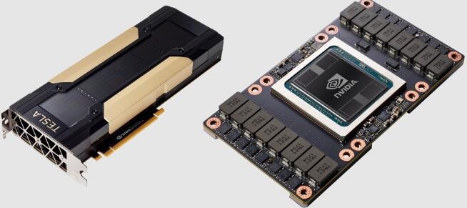
The Nvidia A100 Tensor Core GPU is based on the Ampere architecture and is available in 40GB and 80GB. As the engine of data center platform, the A100 delivers up to 20 times the performance of the previous generation Volta and can be partitioned into seven GPU instances to dynamically adjust to changing needs. And it can achieve excellent acceleration at different scales for AI, data analysis, and HPC application scenarios, effectively helping high-performance elastic data centers.
What’s more, if using automatic mixed precision and FP16, the performance can be further improved up to 2 times. 2048 A100 GPUs can handle BERT-like training workloads at scale in under a minute. For very large models with huge data tables, such as DLRM for recommender systems, A100 80GB provides up to 1.3 TB of unified memory per node and is up to 3x faster than A100 40GB.
For deep learning inference, the A100 can accelerate across the entire precision range from FP32 to INT4. Multi-Instance GPU technology allows multiple networks to run simultaneously on a single A100, and optimize utilization of computing resources.
Intel Loihi 2
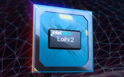
The second-generation neuromorphic chip Loihi 2 released by Intel has an area of 31mm2 and can package up to 1 million artificial neurons, while the previous generation product has an area of 60mm2 and supports 131,000 neurons. It runs 10x faster than the previous generation, is 15x more resource-dense, and is more energy efficient. And it has 128 neuromorphic cores, and each core has 8 times the number of neurons and synapses compared to the first generation, where these neurons are connected to each other through 120 million synapses.
Loihi 2 uses a more advanced manufacturing process-Intel 4, Intel's first EUV process node, and requires only half the space for each core. At the same time, it can not only communicate between chips through a 2D connection grid, but also communicate on a three-dimensional scale, thereby greatly increasing the total number of neurons that can be processed. Further more, the number of embedded processors per chip has increased from three to six, and the number of neurons per chip has increased eight times.
Loihi 2 uses spiking neural networks (SNNs) to solve many problems very efficiently, but it requires make algorithm development in an equally different way. However, most of the people who are proficient in it come from the field of theoretical neurobiology. That is to say, it is only for the research field, which will limit its market scale. Of course, Intel is combining it with the Lava open-source software framework, hoping that Loihi derivatives will eventually appear in a wider range of systems, from acting as coprocessors in embedded systems to large Loihi clusters in data centers.
Google TPUv4
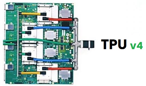
Google's AI chip TPU v4 is 2.7 times faster than TPU v3. By integrating 4096 TPU v4 chips into one pod, it can achieve 1 exaflop-level computing power, which is equivalent to the sum of 10 million laptops, double the world's largest supercomputer. Google uses these systems for its own AI applications (such as search suggestions, language translation or voice assistants), it also opens up the TPU infrastructure to Google Cloud users as cloud services (fee).
The matrix multiplication TFLOP provided by the fourth-generation TPU is more than twice that of the TPU v3, significantly improving memory bandwidth. The performance of the TPU v4 pod is 10 times higher than that of the TPU v3 pod, and it will mainly run on carbon-free energy, which not only calculates faster, but also saves energy.
AWS Trainium
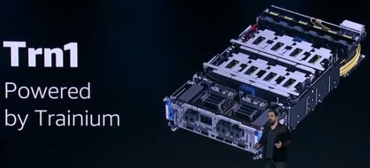
AWS Trainium is the second-generation machine learning (ML) accelerator that AWS purpose built for deep learning training of 100B+ parameter models. It is specially optimized for deep learning training workloads, including image classification, semantic search, translation, speech recognition, natural language processing and recommendation engines, etc., and supports TensorFlow, PyTorch and MXNet, etc. Compared with standard AWS GPU instances, the throughput of EC2 TRN1 instances based on this chip is increased by 30%, which can reduce the inference cost of model by 45%.
In addition to, it shares the same AWS Neuron SDK as Inferentia, which makes it easy for developers using Trainium. And it is available via Amazon EC2 instances and AWS Deep Learning AMIs, as well as management services including Amazon SageMaker, Amazon ECS, EKS, and AWS Batch.
Qualcomm Cloud AI100
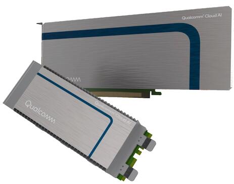
Qualcomm Cloud AI100 inference chip adopts 7nm process, contains 16 sets of AI cores, INT8 inference throughput with 400 TOPS, and 4 @ 64-bit LPDDR4X-4200 (2100MHz) memory controllers, each controller manages four 16-bit channels with a total system bandwidth of 134GB/s.
Qualcomm provides three different packaging forms for commercial deployment, including mature PCIe 4.0 x8 interface, and DM.2 and DM.2e interface (25W / 15W TDP), while the power consumption is: DM.2e @ 15W, DM.2 at 25W, PCIe/HHHL @ 75W.
Esperanto ET-SoC-1
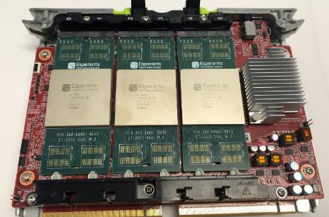
Esperanto's RISC-V-based ET-SoC-1 chip integrates 1,000 cores and is designed for data center AI inference. The chip uses TSMC's 7nm process, built-in 160M byte SRAM, and contains 24 billion transistors.
The core of it includes 1088 ET-Minions and 4 ET-Maxions. Where ET-Minion is a general-purpose 64-bit in-order core with proprietary extensions for machine learning, including vector and tensor operations on up to 256-bit floating-point numbers per clock cycle. And it is the company's proprietary high-performance 64-bit single-threaded core with four-issue out-of-order execution, branch prediction and prefetch algorithms.
Graphcore Colossus Mk2 GC200 IPU
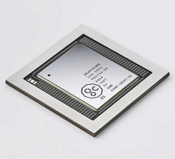
Graphcore’s second-generation IPU chip, Colossus MK2 GC200, adopts TSMC’s 7nm process. The architecture is similar to the previous generation IPU, but the number of cores has increased to 1472 (up to 20%), and its on-chip SRAM has increased to 900MB (3 times more). In terms of interconnect scalability, it is 16 times stronger than the previous generation.
The system solution IPU-M2000 containing four MK2 chips can be expanded to 1024 IPU-PODs, that is, 512 racks. After a cluster of up to 64,000 MK2 chips, its 16bit FP computing power can reach 16 ExaFLOPs. The M2000 device contains a gateway chip inside, providing access to DRAM, 100Gbps IPU-Fabric Links, PCIe interface connected to SmartNIC, 1GbE OpenBMC management interface, and M.2 interface. The performance of M2000 in neural network training is 7-9 times that of the previous generation, and the inference operation is also improved by more than 8 times.
Cerebras WSE-2
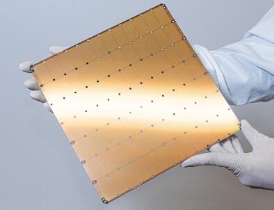
The largest chip ever designed by Cerebras is called the wafer scale engine (WSE). The second-generation chip WSE-2 uses TSMC's N7 process. It has an area of 46225mm2 and contains more than 1.2 trillion transistors, built-in 850,000 cores for optimizing deep learning. Compared with the Nvidia A100 GPU, WSE is more than 56 times larger, with up to 40GB of on-chip memory, up to 20 PB/s of memory bandwidth, and up to 220 PB/s of network bandwidth.
The WSE-2-based AI acceleration system CS-2 greatly increases memory and structure bandwidth while keeping its system power consumption unchanged (23kW). The computing processing performance of a single CS-2 system is equivalent to dozens or hundreds of GPUs, which can reduce the time required to complete the most complex AI workloads from months to minutes.
Ambarella CV52S
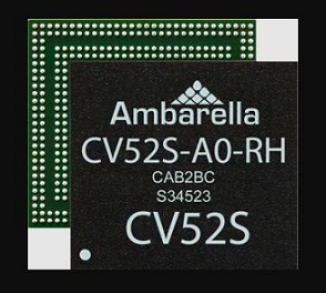
Based on CVflow architecture and advanced 5nm process, the single SoC of CV52S has ultra-low power consumption, and supports 4K encoding and powerful AI processing. The chip adopts dual-core 1.6GHz Arm A76 with 1MB L3 cache; super ISP has excellent wide dynamic range, low light, fisheye correction and rotation processing performance; built-in privacy masking function can shield some shooting scenes; new PCIe and USB 3.2 interface can realize more complex multi-chip security system design; support rock-solid hardware-level digital security technologies such as secure boot, OTP and Arm TrustZone, to ensure the information security of camera equipment; support multiple video stream input, through MIP virtual channel interface can connect up to 14 cameras; support LPDDR4x/LPDDR5/LPDDR5x DRAM.
Compared with the previous generation of chips, CV52S series chips mainly focus on monocular security cameras, support 4K 60fps video recording. Their AI computer vision performance is improved by 4 times, CPU performance is increased by 2 times, and memory bandwidth is increased by more than 50%. While improvements in neural network performance enable more types of AI processing to be performed on edge devices without uploading to the cloud.
Hailo-8
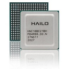
Hailo-8, an edge AI processor from Israeli AI chip company Hailo, has a performance of 26 tera/second (top) and a high performance of 2.8 TOPS/W. According to the company, Hailo-8 outperformed hardware such as Nvidia's Xavier AGX, Intel's Myriad-X and Google's TPU modules in several AI semantic segmentation and object detection benchmarks.
The M.2 module based on Hailo-8 is an accelerator module specifically for AI applications, which can provide up to 26TPOS computing power support, and is suitable for application scenarios such as edge computing, machine learning, and reasoning and decision-making. And it has a full PCIe Gen-3.0 4-lane interface, plugs into existing edge devices with M.2 sockets, and performs inference on a wide range of market segments with real-time and low-power deep neural networks.
Development Trend within 10 Years
The next 10 years will be a new decade of accelerated computing architecture changes. In terms of computing and storage integration, that is, putting the computing unit and the storage unit together increases the computing and data throughput of the AI system and significantly reduces power consumption. Will there be a new type of non-volatile storage device that adds AI computing functions to save data movement operations? Now the computing power of hardware is greater than the performance of data reading and accessing. When the computing unit is no longer the bottleneck, how to reduce the memory access delay will be the focus.
Generally, the closer to the calculation, the faster the memory, the higher the cost per byte, and the more limited the capacity, so new storage structures will emerge as the times require.
The second trend is sparse computing (SC). With the introduction of hundreds of billions to trillions of network models, the model is getting bigger and bigger, but not every neuron can be effectively activated. At this time, SC can effectively reduce useless energy efficiency. Especially in the application of recommendation scenarios and graph neural networks, sparsity has become the norm.
For example, Harvard University proposed an optimized five-stage pipeline structure for this problem, and a trigger signal is output at the last stage. After the activation layer, the necessity of the next calculation is pre-judged. If it is found that this is a sparse node, the SKIP signal is triggered to avoid the useless power consumption of the multiplication operation.
The third trend is to support more complex AI operators. On the basis of standard SIMD, the special structure multiplexing of CNN can reduce the data communication of the bus. The transformer structure needs to switch between calculation and storage for big data, or the dynamic shape that often needs to be supported in the NLP and voice fields. Also reasonably decomposing and mapping operators of these different complex structures to effective hardware has become a direction worthy of research.
The last is faster inference latency and storage bit width. As Apple, Qualcomm, and Huawei have launched AI reasoning hardware IP on mobile phone SoCs, further more, mobile phone SoCs have introduced learnable functions in recent years. How to execute faster on the mobile phones in the future is a point of great concern to the industry. In addition, in terms of theoretical calculations, the bit width of neural network calculations has ranged from 32 bits to 16 bits, and mixed precision has appeared, and now 8 bits, or even lower bits, have gradually entered the field of practice.
AI chip, what will ultimately determine the final success? What about Nvidia's GPU hardware architecture, Huawei’s Da Vinci architecture, and Google’s TPU systolic array architecture? In general, the choice of chip architecture should serve the ecology of the entire chip project, which is the result of the game of many factors. Nvidia can occupy the leading market in the field of AI today, and its underlying hardware architecture, perfect software and hardware connections are inseparable.

 English










