How the new device achieves higher energy efficiency and better thermal performance compared to the previous generation high-current buck-boost μModule regulator.
Many applications require a wide input and/or output voltage range, such as battery-powered systems. When the input voltage may be either lower or higher than the output voltage, the power supply needs to regulate its output voltage. As long as ground isolation is not required, the four-switch buck-boost topology can provide extremely high efficiency and power density for such applications. Additionally, the buck-boost regulator is very versatile and can function as a purely buck power supply or as a boost power supply (with short-circuit protection).
Analog Devices' μModule division has developed several buck-boost regulators. low-current applications. The LTM4607 series, LTM8055 series, and the newly released LTM4712 buck-boost modules support high-current applications (up to 12 A).
The LTM4607/LTM4605/LTM4609 series integrates the controller and MOSFETs, but requires external power inductors and sense resistors (RSENSE) to be connected on the PCB to form a complete power solution, as shown in Figure 1. In contrast, the LTM8054, LTM8055, and LTM8056 integrate the power inductors and RSENSE into the μModule package, simplifying the design and layout for customers, as shown in Figure 2. Compared to the LTM4607 series, the LTM8055 series provides a smaller form factor solution; however, its output current is limited by the smaller integrated inductor, resulting in certain limitations in thermal performance and efficiency.
In 2023, Analog Devices (ADI) released the new high-current, four-switch buck-boost regulator, the LTM4712. This is a 36 VIN (maximum) and 12 A power module, packaged in a high-density 16 mm × 16 mm × 8.34 mm BGA form factor. It utilizes ADI’s proprietary advanced component packaging technology, integrating high-performance power inductors into the package. Figure 3 shows the proprietary current-sensing scheme integrated into the module. This not only saves space but also effectively reduces additional power losses. The device features an advanced buck-boost controller and an advanced ADI package, enabling ultra-high power levels, power density, efficiency, and excellent thermal performance across a wide input-output voltage range.
The LTM4712 features fast cycle-by-cycle current mode control, which helps achieve reliable protection and smooth mode transitions. When configured in parallel to support higher current applications, it enables excellent current sharing functionality. Additionally, this new device supports an optional constant output current mode, which is useful for battery charging applications, and also allows for redundant inputs, enhancing its versatility as a redundant power supply.
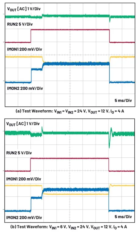
Figure 1: LTM4607 Power Stage Schematic Diagram
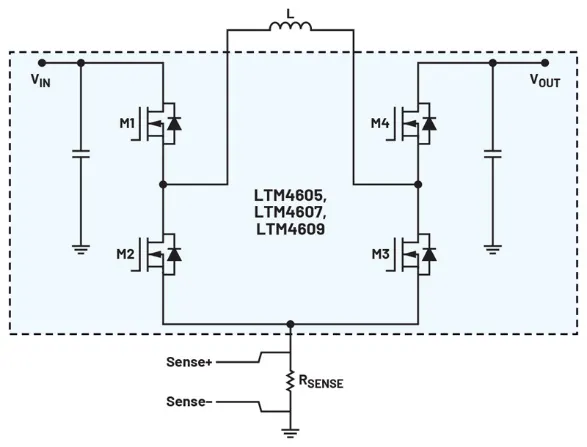
Figure 2: Typical Application Circuit of LTM8055
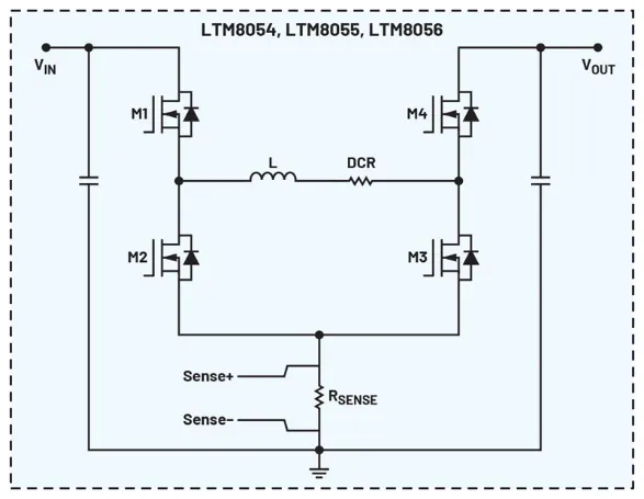
Figure 3: Typical Application Circuit of LTM4712
Efficiency Improvement and Thermal Performance Enhancement
Figure 4 compares the efficiency of the LTM4607, LTM8055, and LTM4712 under 6 V VIN, 12 V VIN, 24 V VIN, and 12 V VOUT conditions. The evaluation used standard evaluation boards that are available for online purchase. According to the test results, the LTM4712 significantly outperforms the other two products in terms of efficiency and offers greater current capability.
Under 12 V VIN and 12 V VOUT conditions, the LTM4712, compared to the LTM8055, delivers double the power while maintaining a 30°C lower temperature. For applications requiring 12 A of current, using the LTM8055 may require paralleling two to three devices, depending on the cooling system. However, with the LTM4712, a single device is sufficient, greatly reducing PCB space and simplifying the circuit design.
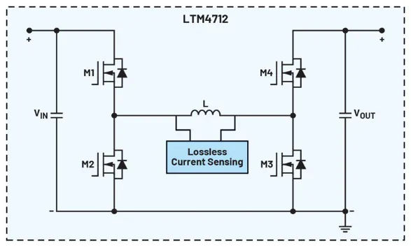
Figure 4: Efficiency Comparison Between LTM4712, LTM4607, and LTM8055
Achieving Good Current Sharing in Parallel Configuration
The LTM4712 supports parallel configurations, enabling higher output power with simple setup. Thanks to its current mode control, it offers excellent current sharing performance. The EVAL-LTM4712-A2Z evaluation kit demonstrates the operation of four modules running in parallel, providing a total output current of 48 A.
When using this device in a parallel configuration, it is necessary to refer to the design and configuration of the evaluation board. To achieve effective current balancing, the COMP and FB pins need to be connected when paralleling the modules. The PHMODE pin can be used to configure the phase shift. In the case of four modules in parallel, connecting the PHMODE pin to INTVCC can generate a 90° phase shift, resulting in excellent interleaving effects. Additionally, to achieve frequency synchronization, the CLOCKOUT signal of the first module should be connected to the SYNC pin of the second module.
Optional constant current regulation
The LTM4712 can be used as a constant output current source, making it suitable for applications such as battery chargers or LED drivers. The load current is set through the ISET pin and an external output current sensing resistor located near the output. The formula VSENSE = IOUT × RSENSE_IOUT defines the voltage representing the average output current. The maximum VSENSE is determined by the voltage on the ISET pin, which ranges from 0.2 V to 1.2 V, corresponding linearly to 0 mV to 50 mV. The ISET pin voltage (VISET) is determined by a 15 μA internal current source and a resistor (RISET) connected between the ISET pin and ground, expressed as VISET = 15 μA × RISET. Therefore, the output current calculation formula is: IOUT = (VISET - 0.2 V)/(20 × RSENSE_IOUT).
It is important to note that when the ISET pin is left floating or when the ISET pin voltage exceeds 1.2 V, the internal circuit will limit the maximum VSENSE to 50 mV. Due to the presence of ripple current in the output, an RC filter should be used on the ISP and ISN pins to achieve accurate average current detection. Additionally, when selecting the feedback resistor between the FB pin and ground, it is essential to ensure that the output voltage it generates is higher than the target VOUT.
Redundant power supply
The LTM4712 supports applications that require redundant inputs. It can be used in systems that require a backup power source or those that draw power from different input sources to support a common load. Figure 5 shows a sample circuit where two modules are powered by different inputs (VIN1 and VIN2) and together provide a 12 V output for a 24 A load. It is important to note that any drop in input voltage will not affect output regulation, and peak inductor current balancing remains effective through the connection of the COMP pin.
Figure 6 shows the test waveforms under two different conditions. Figure 6a illustrates the case where both phase 1 and phase 2 are operating in buck-boost mode. Initially, phase 1 provides a 4 A load current. After phase 2 is activated, both phases gradually share half of the load current. The IMON waveform shows that when both phases are running, the load current is evenly shared between the two phases.
Figure 6b shows the case with the same load condition but different inputs. Here, phase 1 operates in boost mode, while phase 2 operates in buck mode. Since the COMP pins are connected together, the peak inductor current of both phases is the same. As a result, the output current of phase 1 (boost) is lower than that of phase 2 (buck). The specific load current provided by each phase can be calculated based on parameters such as inductance, switching frequency, VIN, VOUT, and total load current. In this example, phase 1 provides 1.4 A of load current, while phase 2 provides 2.6 A of load current.
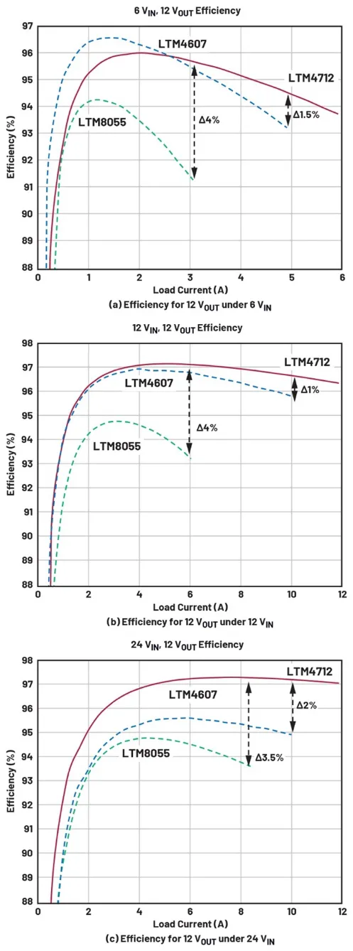
Figure 5: Redundant input application circuit
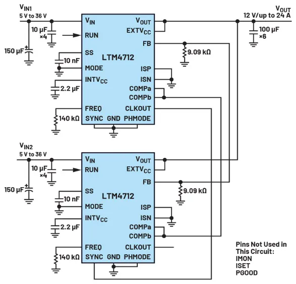
Figure 6: Redundant input application circuit
Conclusion
The LTM4712 not only easily supports parallel configurations for higher power applications but also demonstrates excellent current balancing in parallel setups. The device can be flexibly configured for constant current output, making it ideal for battery charging systems or LED applications. Furthermore, it supports redundant inputs, further enhancing its adaptability.

 English










