Abstract
The third part of this series of articles describes a simple loop compensation design method for current-mode-controlled switching power supplies. This control architecture is widely used in power management solutions, including many of ADI’s power products. It supports the use of a simple Type 2 compensation network to design and optimise the power supply feedback loop, ensuring fast transient response and ample stability margin. This article introduces fundamental loop design concepts, clearly explains the Type 2 compensation network, and explores the role of each compensation component. The loop design process can be simplified into three straightforward steps. Furthermore, the LTpowerCAD® design tool can further simplify the loop design and optimisation process.
Introduction – Basic Concepts
Switching power supplies are widely used in modern electronic systems, offering high efficiency and high power density. For inexperienced systems engineers, optimising the design of power loop compensation can be a critical yet challenging task. Most of ADI’s switching regulators employ a current-mode control architecture to achieve high performance and reliability. For example, Figure 1 shows a basic block diagram of a common current-mode-controlled buck converter. This architecture comprises an internal current detection loop and an external output voltage regulation loop. The internal current detection loop forces the inductor current to track the output voltage of the compensation network at the ITH node; thus, the inductor effectively becomes a current source controlled by the output VITH of the voltage loop error amplifier. Consequently, the buck converter power stage, including the current loop, behaves as a single-pole system at frequencies below the current loop bandwidth. Therefore, a simple Type 2 compensation network is sufficient to optimise the power loop stability and transient performance. In Figure 1, the Type 2 compensation network is exemplified by the RTH, CTH and CTHP network on the ITH pin, which is the output of the error operational amplifier.
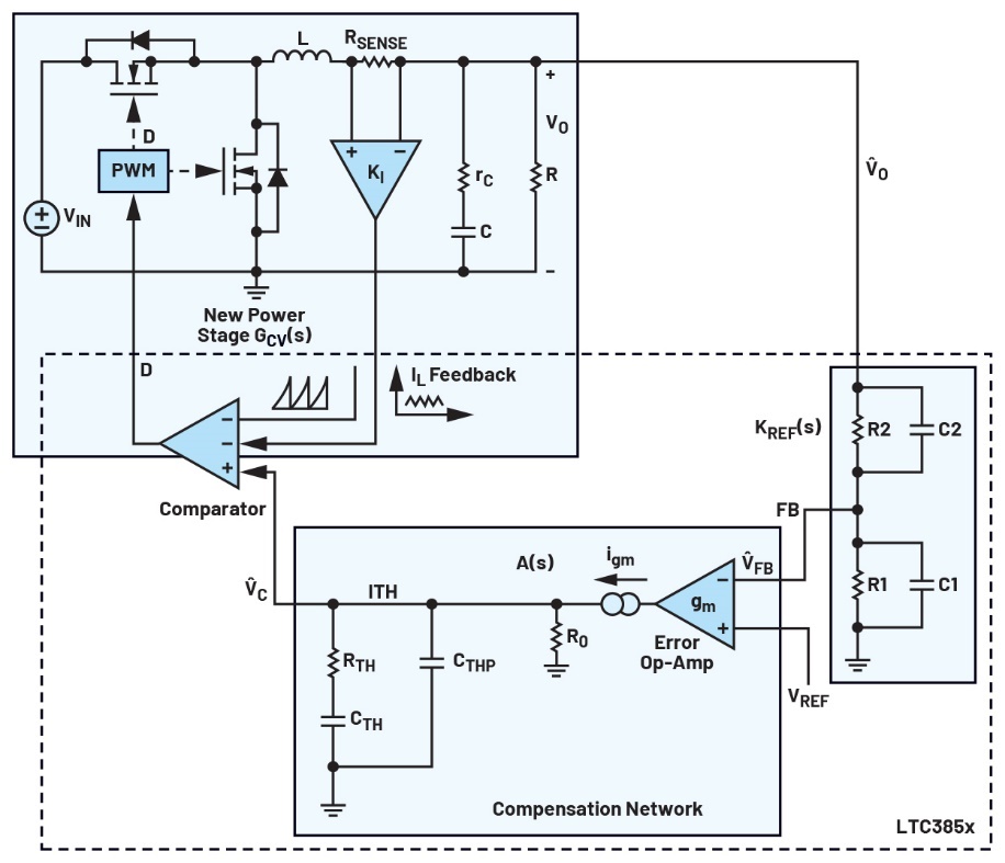
Figure 1. Block diagram of a peak-current-mode buck converter, comprising an internal current loop, an external voltage regulation loop and a Type 2 compensation network on the ITH pin.
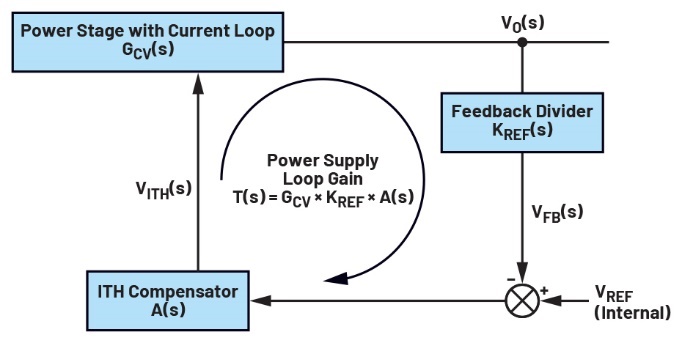
Figure 2. Schematic diagram of the power loop gain.
Figure 2 shows a conceptual diagram of the power loop gain. KREF is the gain of the feedback resistor divider network from the power supply output VO to the FB pin. A(s) is the gain of the voltage loop compensation error amplifier network from the FB pin to the ITH pin. GCV(s) is the power stage transfer function from the error amplifier output node VITH to the power supply output voltage VO, including the internal current loop. Therefore, the total power supply loop gain T(s) can be calculated using Equation 1:

Design and Optimisation Objectives for Switch-Mode Power Supply Loops
An optimised power supply loop design should feature high loop bandwidth to achieve fast transient response whilst maintaining sufficient stability margin. Furthermore, in switching power supplies, it is essential to attenuate switching noise in the feedback loop to minimise switching waveform jitter. In summary, the key objectives of power supply loop design are as follows:
1. Loop bandwidth (fBW): To achieve a fast transient response, the higher the loop bandwidth, the better; however, in practical applications, it is limited by the switching frequency (fSW). Typically, the maximum bandwidth is set to 1/10 or 1/5 of fSW.
2. Phase margin: A phase margin greater than 45° is generally required, and a margin greater than 60° is recommended.
3. Gain margin: The gain margin is defined as the gain attenuation at a loop phase of –180°, and it should be at least 8 dB to 10 dB.
4. Switching noise attenuation margin: For current-mode controlled switching power supplies, switching noise in the feedback loop must be attenuated to minimise jitter in the switching node waveforms. In practical applications, the attenuation at fSW/2 should ideally be greater than 8 dB.
An intuitive understanding of Type 2 compensation networks
In order to design and optimise a compensation network, power supply designers first need to understand how the R or C values of each compensation element affect the loop gain and the load transient response. As shown in Figure 3, a Type 2 compensation network comprises: a typical transconductance error amplifier (i.e. a voltage-controlled current source) with a gain of gm; the amplifier’s parasitic output resistance R0; and a compensation network comprising RTH, CTH and CTHP. These three key R/C components at the ITH pins are used to adjust the compensation gain A(s), thereby determining the power supply loop’s gain bandwidth, stability margin and transient response performance.
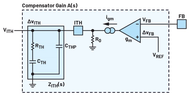
Figure 3.2: Type 3.2 compensation network and its gain A(s).
The definition of compensation gain A(s) is given in Equation 2.

For a given controller IC, the internal gm and R0 are fixed; therefore, the impedance ZITH(s) of the network comprising RTH, CTH and CTHP determines the compensation gain A(s). ADI Application Note AN149 provides a detailed derivation of the formula (see Equation 3): 1
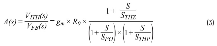
among which
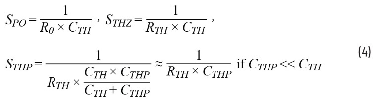
Power supply designers do not need to memorise this A(s) formula; instead, they can gain an intuitive understanding of the compensation gain simply by observing how the ZITH impedance varies with frequency, as illustrated by the conceptual curve in Figure 4.
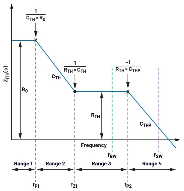
Figure 4. Conceptual Bode plot of the ZITH(s) (including RO) amplitude versus frequency (CTH>>CTHP).
With regard to the conceptual curve in Figure 4, viewed from left to right, the frequency increases from a lower value to a higher value and can be divided into the following ranges:
Range 1: From DC to the low-frequency pole fP1, all capacitors are treated as high-impedance open circuits. Consequently, the magnitude of ZITH is determined by the parasitic output resistance RO of the error amplifier, which is typically a very large value (of the order of MΩ). Within this range, the error amplifier A(s) exhibits a flat, high DC gain equal to gm × R0.
Range 2: As the frequency increases, the impedance of the first CTH capacitor begins to decrease (note that CTH >> CTHP, so the CTHP impedance remains very high). At frequency fP1, the magnitude of the CTH impedance is comparable to RO. Beyond fP1, as the frequency increases further, the CTH impedance determines the total ZITH impedance.
Range 3: As the frequency increases further, the magnitude of the CTH impedance eventually drops to a value close to that of RTH in the series path. Thereafter, the RTH value dominates the total ZITH value, keeping it flat within this range. The cut-off frequency at which the CTH and RTH impedance values are close to each other is defined as the ‘zero-point frequency fZ1’. The target power loop bandwidth fBW is typically set within frequency range 3.
Range 4: As the frequency increases further, the smaller parallel CTHP impedance eventually drops to a value comparable to that of RTH. Thereafter, the ZITH magnitude is determined by the CTHP impedance. The cut-off frequency at which the RTH and CTHP impedances are close to each other is defined as the “second high-frequency pole fP2”. Where required, this high-frequency pole should be located below the power supply switching frequency fSW to attenuate switching noise.
The above indicates that, across different frequency ranges, the magnitude of the ZITH impedance is determined by each individual R or C component. This phenomenon helps us understand the influence of each component on the power loop gain and transient response.
How do the various compensation components affect loop gain and transient response?
(1) Compensation resistor RTH
Typically, the compensation network is designed such that the power loop bandwidth fBW lies between the zero fZ1 and the pole fP2 within the frequency range 3. Within this range, the ZITH magnitude is determined by the value of RTH. In other words, the value of RTH directly determines the power loop bandwidth fBW. Figure 5 illustrates that increasing the value of RTH enhances the compensation gain A(s) between fZ1 and fP1. Consequently, the higher the value of RTH, the higher the loop bandwidth, as shown in Figure 6a. Increasing the loop bandwidth typically reduces the undershoot and overshoot amplitudes of the supply voltage VOUT during load transients, as shown in Figure 6b, whilst the VOUT settling time following a transient event remains largely unchanged.
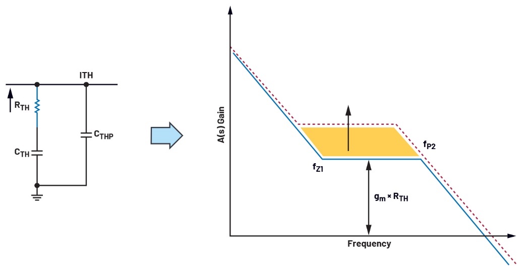
Figure 5. Increasing RTH increases the compensation gain A(s) between fZ1 and fP2.
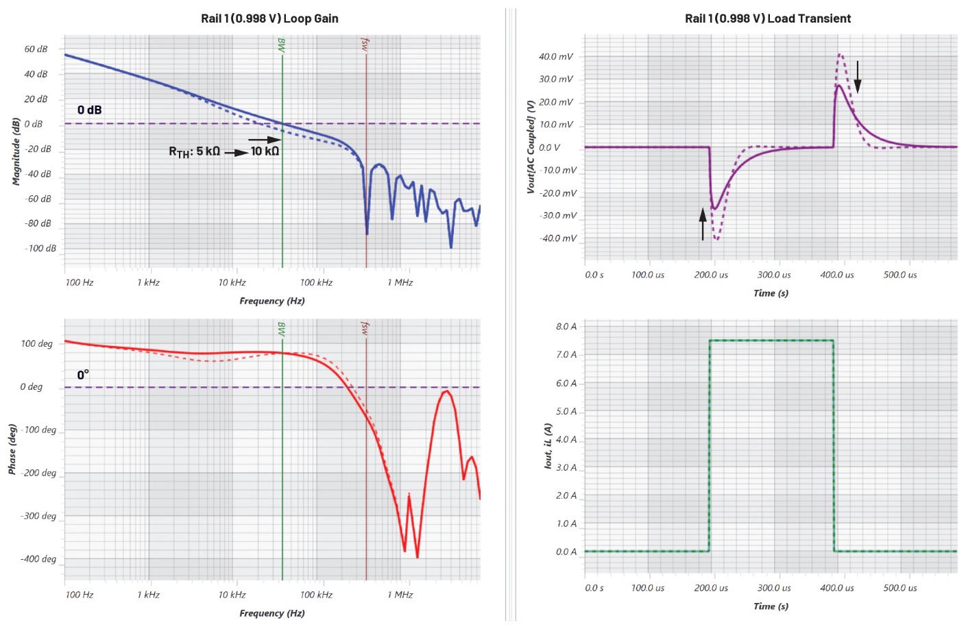
Figure 6. Adding an RTH increases the bandwidth of the power loop, thereby reducing VOUT undershoot and overshoot during load transients.
(2) Compensation capacitor CTH
In a typical design, the compensation capacitor CTH should only affect the loop gain in frequency range 2, between fP1 and fZ1. Figure 7 shows that reducing the CTH value (higher impedance) increases the A(s) gain in frequency range 2. Figure 8 shows that reducing CTH does not affect the power supply loop bandwidth; therefore, it has little effect on the magnitude of VOUT undershoot and overshoot during load transients. However, CTH has a higher gain in the lower frequency range 2, so a smaller CTH helps to shorten the transient settling time.

Figure 7. Reducing CTH increases the compensation gain A(s) in frequency band 2 between fZ1 and fP1.
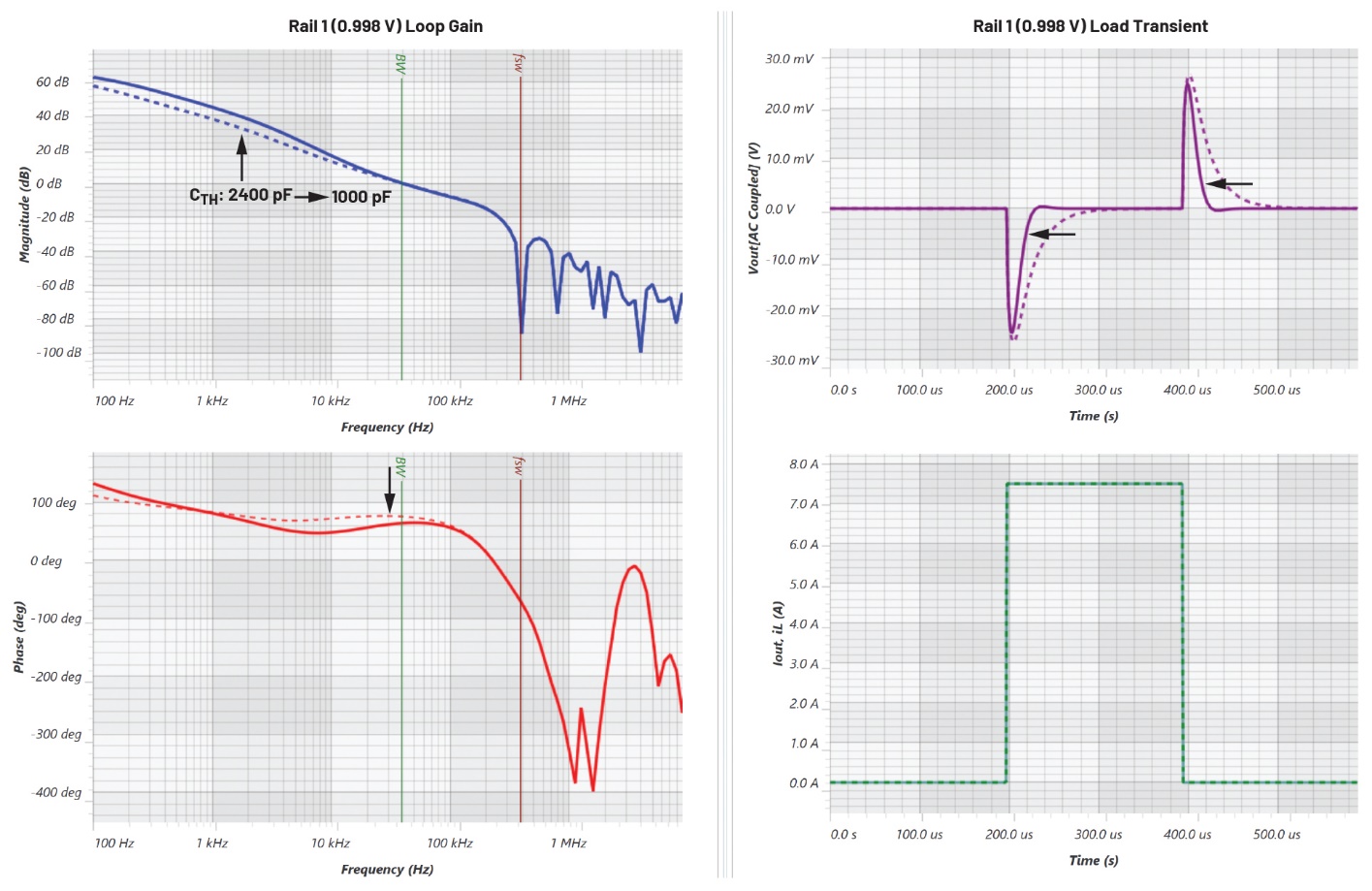
Figure 8. Reducing the CTH increases the power loop gain at lower frequencies, thereby shortening the VOUT settling time during load transients without affecting the VOUT undershoot or overshoot peaks.
(3) Compensation Capacitor (CTHP)
CTHP typically employs a small, high-frequency, low-ESR, low-ESL capacitor to attenuate high-frequency noise in the feedback loop, thereby ensuring clean and low-jitter switching waveforms. Such a capacitor is particularly beneficial for current-mode power supplies that are highly susceptible to noise at the current comparator input. CTHP should be significantly smaller than CTH and is effective only at high frequencies (Range 4). With regard to the power loop gain, CTHP helps achieve the required attenuation of 8 dB or more at fSW/2. Figure 9 illustrates how increasing CTHP helps reduce the A(s) gain at higher frequencies. Figure 10 demonstrates that increasing CTHP reduces the power loop gain at higher frequencies, thereby attenuating high-frequency noise. Provided that CTHP is kept to a small value (<
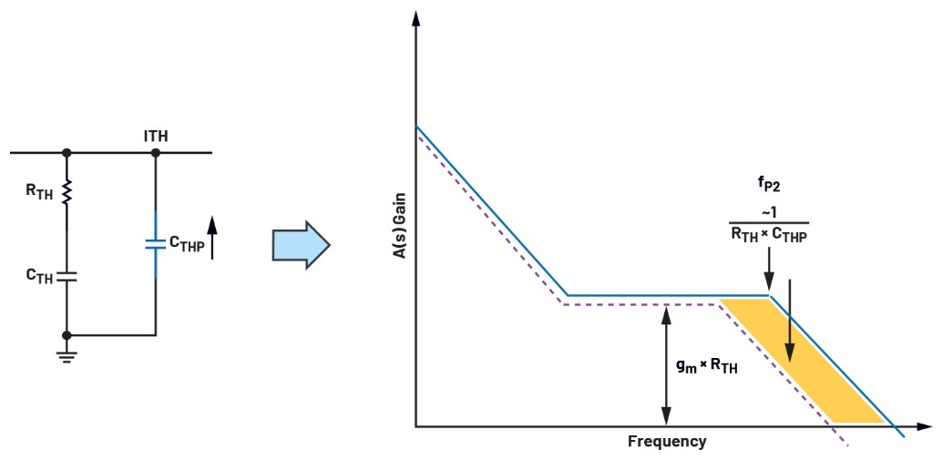
Figure 9. At higher frequencies, the CTHP attenuates both gain and noise.
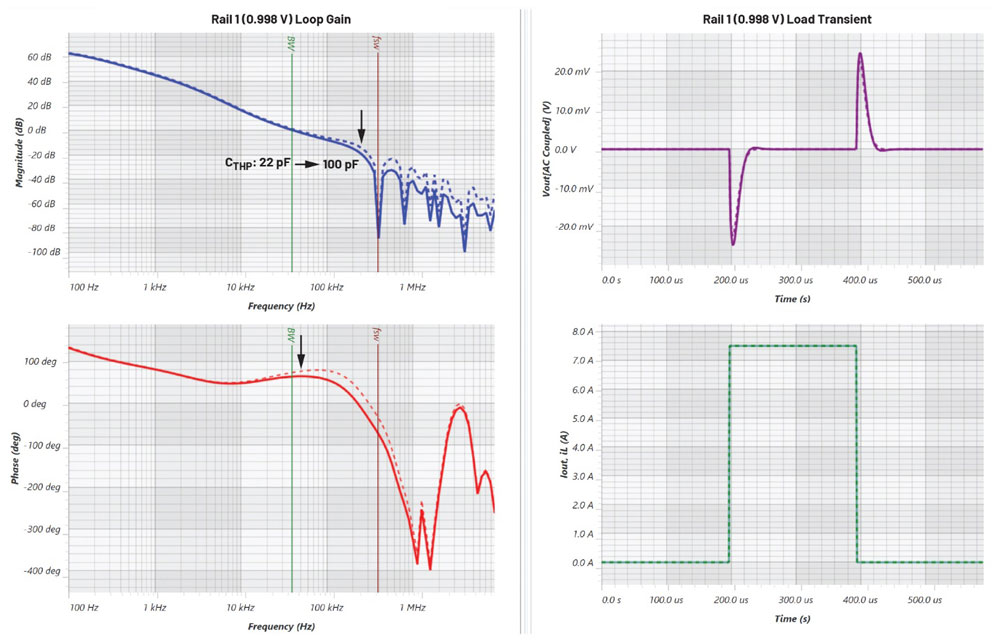
Figure 10. A suitably designed CTHP value can attenuate high-frequency loop gain whilst having a negligible effect on the power supply’s transient response.
A simple three-step process for loop compensation design
Once you have a clear and intuitive understanding of ZITH networks, you can complete a Type 2 compensation design for a given target loop bandwidth in just three simple steps. Designers can use the LTpowerCAD power design tool or a benchtop Bode plotter for the design.
Step 1: Set the RTH value for the target loop bandwidth
Conceptually, for a given target loop bandwidth fBW, the RTH value can be calculated directly using Equation 1. At the loop bandwidth (crossover frequency), the loop gain is 0 dB, i.e. 1:

The RTH value can therefore be calculated as follows:


In practice, if it is not convenient to estimate the GCV value using a typical controller IC, ADI’s LTpowerCAD software can be used as an alternative. LTpowerCAD is a comprehensive power supply design tool that supports optimisation of the power stage and loop compensation². On the LTpowerCAD loop design page, users can first preset a very large CTH value, then start with a small RTH value and gradually increase it until the target loop bandwidth is achieved. In this scenario, when employing current-mode control, the phase margin should ideally exceed 60°. If the margin is insufficient, simply reduce the RTH value to lower the loop bandwidth until the required 60° phase margin is achieved. See Figure 11.

Figure 11. Step 1 of loop design: Set a relatively high CTH value, then increase RTH gradually from low to high until the target power supply bandwidth is achieved.
If LTpowerCAD is not used and the laboratory employs Bode plot measurement equipment, designers can still start with a higher CTH value and then increase RTH from a very small value to a large one until the required loop bandwidth and phase margin are achieved in the measurements.
Step 2: Set the CTHP value to attenuate noise
Next, using the LTpowerCAD tool or Bode plot measurements, the CTHP should be increased from 0 until the loop gain at fSW/2 is less than –8 dB, thereby achieving the attenuation of switching noise. Furthermore, the power supply gain margin (when the phase margin is 0) should also be between 8 dB and 10 dB. See Figure 12.
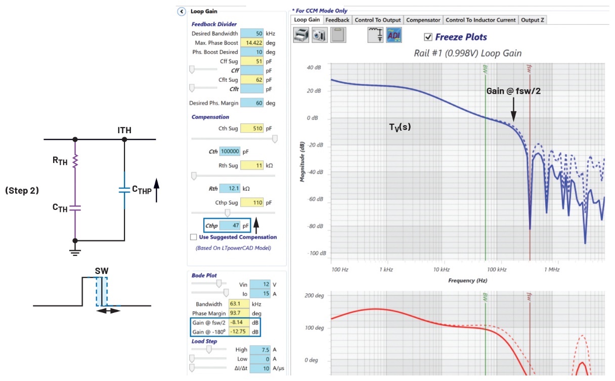
Figure 12. Step 2 of loop design: The CTHP is increased from 0 until an 8 dB attenuation in loop gain is achieved at fSW/2.
Step 3: Set the CTH value to achieve fast transient settling time
In this step, the very high default CTH value should be reduced until the power supply’s phase margin begins to decrease noticeably, indicating that fZ1 is approaching the loop bandwidth. A smaller CTH helps to shorten the load transient settling time. However, if the CTH is set too low, it will ultimately affect the power supply’s phase margin. A phase margin of 45° to 60° should be maintained. See Figure 13.
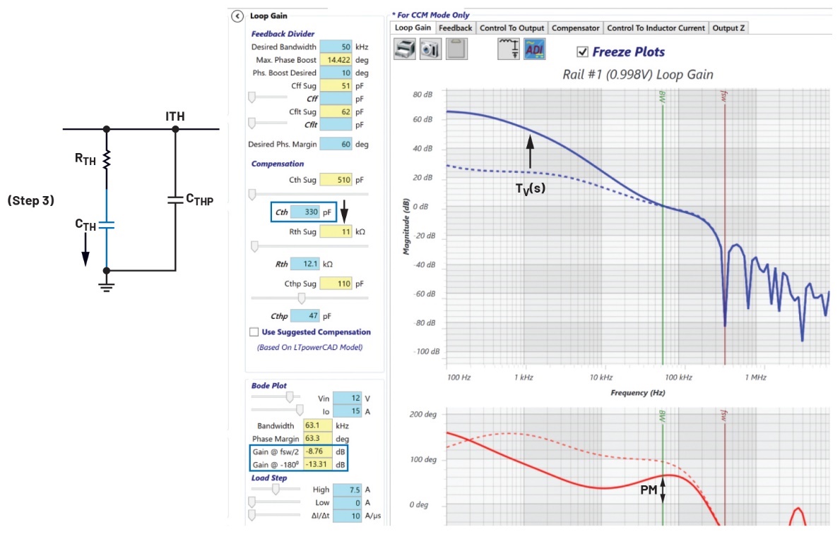
Figure 13. Step 3 of the loop design: Reduce the CTH value to shorten the transient time until the power supply phase margin begins to fall to the required value of 60°.
(Optional) Step 4: Achieve further phase improvement via the resistor divider capacitor
If adjusting CTH, CTHP and RTH still fails to achieve the required loop bandwidth and stability margin, a feedforward capacitor (CFF) and a filter capacitor (CFLT) can be added to further adjust the resistor divider network. The purpose of this step is to improve the phase around the target loop bandwidth, which is typically achieved using CFF. This can be accomplished in the LTpowerCAD loop compensation page by opening the Feedback tab. Figure 14 shows correct and incorrect examples of resistor divider capacitor design. The correct example significantly improves the phase at the target loop bandwidth frequency.
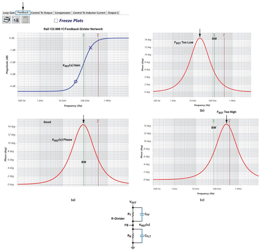
Figure 14. Optional additional steps: Adjusting phase gain using a feedback resistor divider network: (a) Optimal design; (b) Phase gain frequency too low; (c) Phase gain frequency too high.
Further simplifying design with LTpowerCAD’s one-click loop design
To further simplify the loop design process, ADI’s LTpowerCAD software offers a one-click automatic loop compensation design function based on the three-step method described in this article. As shown in Figure 15, users can set the target loop bandwidth—typically within the range of 1/10 to 1/5 of the switching frequency—and then tick the ‘Use Suggested Compensation’ checkbox. The LTpowerCAD programme will provide a set of RTH, CTH and CTHP values to achieve the target loop bandwidth and good phase margin. If the target bandwidth or phase margin cannot be achieved, the user may manually reduce the target loop bandwidth frequency. If the user does not wish to use this one-click loop design feature, but prefers to manually design and fine-tune the loop and load transient performance, they may deselect the “Use Suggested Compensation” checkbox to disable this function.
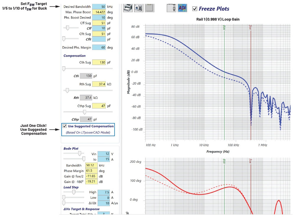
Figure 15. Using the ‘Use Suggested Compensation’ option in the ADI LTpowerCAD design tool to complete automatic loop compensation design with a single click.
Conclusion
For switching power supplies employing common current-mode control architectures, the simple three-step method described in this article allows for the straightforward completion of loop compensation design and optimisation. The LTpowerCAD design tool provides real-time results, and its one-click automatic loop design function greatly simplifies the design and optimisation process.

 English