STM32 ADC Basic
Block Diagram Brief
The STM32 ADC has 18 input channels, which correspond to 18 input multi-channel switches. After the input signal selected, it goes to the voltage comparator, which can judge the two input signal voltages and output a high or low level. Its two input terminals, one is the voltage to be measured, and the other is the voltage output terminal of the DAC. The process of voltage regulation is completed by successive-approximation register (SAR). To find the code of the unknown voltage as quickly as possible, it usually uses the dichotomy method.
EOC (End Of Convert) is the conversion end signal, START is the start of conversion. Give an input pulse, and start the conversion. CLOCK is the ADC clock, because the ADC is judged step by step, so the clock is needed to drive this process. The following VREF+ and VREF-is the reference voltage of the DAC. For example, giving a data of 255, whether it corresponds to 5V or 3.3V is determined by the reference voltage. The reference voltage of the DAC also determines the input range of the ADC, so it is also the ADC reference voltage. The left is the power supply of the chip circuit, VCC and GND, usually the VCC of the reference voltage is the same and will be connected together. In addition, the negative pole of the reference voltage and GND are also the same and connected together. Generally, the range of the ADC input voltage is the same as that of the power supply.
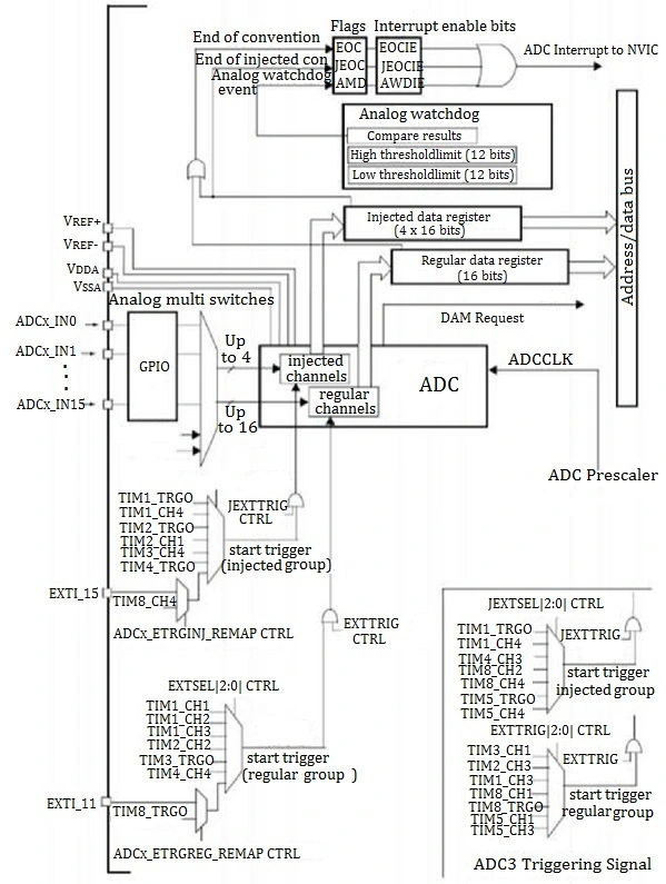
Figure 1: STM32 ADC Block Diagram
ADC Regular Group and Injected Group
Working Principle
On the left is the input channel of the ADC, including 16 GPIO ports, IN0~IN15, and two internal channels, one is the internal temperature sensor, the other is VREFINT, the internal reference voltage, a total of 18 input channels. Then reach the analog multi-channel switch, you can specify the desired channel, the right is the output. Enter the ADC converter, the conversion result will be placed in the data register, so you can get the data from here. For ordinary ADCs, only selects a channel, starts conversion, waits for the conversion to complete, and retrieves the result. This is a common process, but STM32 can select multiple at the same time. At the time, it is also divided into two groups, the regular group and the injected group.
The regular group can select up to 16 channels at a time, and the injected group can select up to 4 channels, just like going to a restaurant to order food. For ordinary ADCs, you order a dish, the chief cooks it for you, and then gives it to you when it is ready. For SMT32 ADC, you take a menu, this menu can be filled with up to 16 dishes, and then the chief will prepare them according to the order of the menu, and serve them to you at one time, so that the efficiency can be greatly improved. Of course, the menu can be only one dish, so that the menu will be simplified into a normal mode.
There are also two kinds of ordinary menus, one is the rule group menu, which can serve 16 dishes at the same time, but the group has only one data register, that is, the table is relatively small, and only one dish can be placed at most. If 16 dishes are served, the first 15 dishes will be squeezed out, only the 16th dish, at this time, if necessary, it is best to cooperate with DMA. DMA is a helper for data transfer. It can move this dish to other places to prevent it from being overwritten. Although the regular group can convert 16 channels at the same time, the data register can only store one result. If you don't want the previous results to be overwritten, take the results away as soon as possible after the conversion is complete.
The injected group is equivalent to a VIP seat in a restaurant. You can order up to 4 dishes at a time on this seat, and there are 4 data registers that can serve 4 dishes at the same time. So you don’t have to worry about data coverage. In reality, it is enough to use the regular group with DMA.
For the regular group, the lower left corner is the trigger part. There are two signals for STM32 ADC trigger. One is software trigger, which is to call a code in the program to start the conversion. The other is hardware, and the trigger source is mainly from the timer, which can be connected to peripherals such as ADC and DAC for triggering conversion). ADC often needs to be converted once in a fixed period of time, such as once every 1ms. The normal idea is to use a timer to apply for an interrupt every 1ms, and manually enable an interrupt. However frequent interrupts have a certain impact on the program. Because they will affect the execution of the main program, and between different interrupts, due to the different priorities, some interrupts will not be able to respond in time, which will affect the ADC convention.
For the above situation, you can use timer. Set a time of 1ms for TIM3, select the update event of TIM3 as TRGO output, and for ADC, select the TRGO of the trigger signal TIM3, so that the update event of TIM3 can automatically trigger the ADC conversion. Because of the timer trigger, the whole process does not need to enter the interrupt, or you can also choose an external interrupt trigger pin to do that. The upper left corner is VREF+, VREF-, VDDA and VSSA. VREF+, VREF- are the reference voltage of the ADC, which determine the range of the ADC input voltage, VDDA and VSSA are the ADC power pins. In general, VREF+ should be connected to VDDA, and VREF- should be connected to VSSA.
VDDA and VSSA are the power supply of the internal analog part, such as ADC, RC oscillator, phase-locked loop, etc. In STM32, VDDA is connected to 3.3V, and VSSA is connected to GND, so the input voltage range is 0~3.3V, and the ADCCLK on the right is ADC clock, used to drive the internal successive comparison clock from the ADC prescaler, which comes from the RCC. The APB2 clock is 72MHz, and then frequency-divided by the ADC to obtain ADCCLK, the maximum is 14MHz. In addition, the divide-by-6 result is 12MHz and the divide-by-8 result is 9MHz.
The above is the DMA request, which is used to trigger the DMA for data transfer, and the above are two data registers. On the top is the analog watchdog, which can store a high threshold limit and a low threshold limit. If the analog watchdog is enabled and its channel is specified. Once the limit exceeded, it will apply for an analog watchdog interrupt on it, and finally lead to the NVIC. For the rule group and injection group, after their conversion completed, there will also be a signal of EOC conversion completion. EOC is the signal for the completion of the rule group, and JEOC is the signal for the completion of the injection group. These two signals will set a flag in the status register. Read this flag, you can know whether the conversion is over. At the same time, these two flags can also go to the NVIC to apply for an interrupt. If the channel corresponding to the NVIC is enabled, they will trigger an interrupt.
Channel Selection
Table 1: Possible Options for Trigger Inputs ADC1, ADC2 & ADC3
|
Channel
|
ADC1
|
ADC2
|
ADC3
|
|
Channel 0
|
PA0
|
PA0
|
PA0
|
|
Channel 1
|
PA1
|
PA1
|
PA1
|
|
Channel 2
|
PA2
|
PA2
|
PA2
|
|
Channel 3
|
PA3
|
PA3
|
PA3
|
|
Channel 4
|
PA4
|
PA4
|
PF6
|
|
Channel 5
|
PA5
|
PA5
|
PF7
|
|
Channel 6
|
PA6
|
PA6
|
PF8
|
|
Channel 7
|
PA7
|
PA7
|
PF9
|
|
Channel 8
|
PB0
|
PB0
|
PF10
|
|
Channel 9
|
PB1
|
PB1
|
-
|
|
Channel 10
|
PC0
|
PC0
|
PC0
|
|
Channel 11
|
PC1
|
PC1
|
PC1
|
|
Channel 12
|
PC2
|
PC2
|
PC2
|
|
Channel 13
|
PC3
|
PC3
|
PC3
|
|
Channel 14
|
PC4
|
PC4
|
-
|
|
Channel 15
|
PC5
|
PC5
|
-
|
|
Channel 16
|
Temperature Sensor
|
-
|
-
|
|
Channel 17
|
Internal Reference Voltage
|
-
|
-
|
Dual ADC Mode: ADC1 and ADC2 work together, and can form synchronous mode, cross mode and other modes. Among them, cross mode means that ADC1 and ADC2 cross to sample a channel, which can increase the sampling rate.
STM32 ADC Configuration
ADC Conventions and Settlement
Regular Group Conversions
1) Single Conversion Mode (Figure 2)
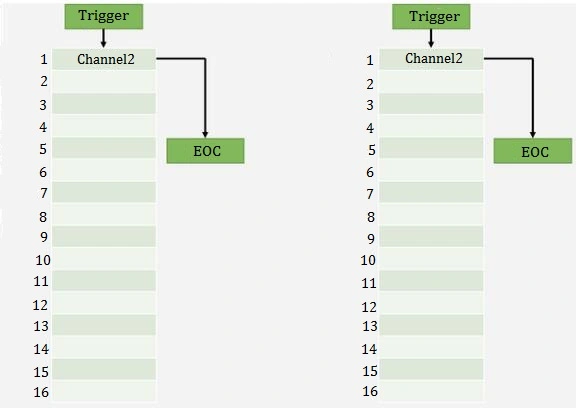
Without scanning, only sequence 1 is valid in the first position. At this time, you simply need to select one but not select a group. We can specify the position we want to convert in the position of sequence 1, such as channel 2, and then the conversion can be triggered, and the ADC will work on this channel 2. After a while, the conversion is completed, the result is placed in the data register, and the EOC flag is set at the same time. The entire conversion process is over.
Judging this flag bit, if the conversion completed, the result can be read in the data register. If you want to start another conversion, you need to trigger it again. That is, repeat the previous operations.
2) Continuous Conversion Mode (Figure 3)
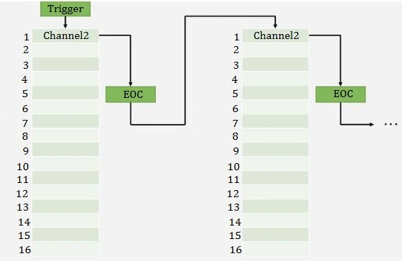
Unlike the above single conversion, it will not stop after one conversion, but immediately continue the next round. So that it only needs to be triggered once, and repeat automatically. The advantage of this mode is that there is no need to wait for a period of time after starting the conversion, it is always converting. There is no need to judge whether it is over. And when you want to read the AD value, just take it directly from the data register.
3) Single Conversion in Scan Mode (Figure 4)
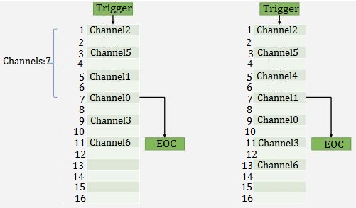
This is the single conversion mode plus scanning. It will use the menu list, for example, the first dish is channel 2, the second dish is channel 5, etc. That is, the number of channels for each position can be specified arbitrarily, and can also be repeated. Setting a parameter in the initialization structure, which is the number of channels, because these 16 positions do not need to be used up. For example, if you specify channel 7 here, it will only look at the first 7 positions, and then after each trigger, it will perform AD conversion on them in turn, and the conversion results will be placed in the register. In order to prevent the data from being overwritten, it is necessary to use DMA to remove the data in time. After the conversion of the 7 channels is completed, an EOC signal is generated, and then the next turn is triggered to start a new conversion.
4) Continuous Conversion in Scan Mode (Figure 5)
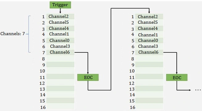
This is the continuous conversion mode plus scanning. In the case of scanning mode, there is also a mode on the right, called intermittent mode. Its function is to pause every few conversions during the process, and it needs to be triggered again to continue.
Trigger Control
This table is the trigger source of the regular group. There are signals from timers and pins. Specifically, pins or timers need to be determined by AFIO remapping. And finally is software bits, where trigger signals can be configured by configuring the registers on the right to complete, and the library function only needs to set a parameter.
Table 1: Internal Trigger Source for Regular Channels
|
Trigger Source
|
Type
|
EXTSEL(2:0)
|
|
TIM1_CC1 Event
|
Internal signal from on-chip timers
|
000
|
|
TIM1_CC2 Event
|
001
|
|
TIM1_CC3 Event
|
010
|
|
TIM2_CC2 Event
|
011
|
|
TIM3_TRGO Event
|
100
|
|
TIM4_CC4 Event
|
101
|
|
EXTI11/TIM8_TRGO Event
|
External pin/internal signal from on-chip timers
|
110
|
|
SWSTART
|
Software Bit
|
111
|
Data Alignment
Regular Group
 (Align Left)
 (Align Right)
This ADC is 12-bit, but this data register is 16-bit, so there is a problem of data alignment. There is two alignment methods: data right alignment, and data left alignment. The former means that the 12-bit data is leaned to the right, and the extra digits of the high digits are filled with 0. The latter means that the 12-bit data is leaned to the left, and the extra digits of the lower digits are filled with 0. Generally, we often use data right alignment, so reading result is directly the conversion result.
If choose data left alignment, the obtained data will be larger than the actual one when read it directly, because the left alignment of the data actually means shifting the data to the left 4 times. For binary data, shifting the data to the left once is equivalent to multiplying the data by 2. Shifting left 4 times is equivalent to multiplying the result by 16, so the direct reading will be 16 times larger than the actual value. When high resolution is not needed, you can choose left alignment and then lower 4 bits are removed, the 12-bit ADC degenerates into an 8-bit one.
Conversion Time
The steps of AD conversion: sampling, holding, quantization, encoding.
The total conversion time of the STM32 ADC is: Tconv = sampling time (the larger the sampling time, the less interference from some glitch signals) + 12.5 ADC cycles (the time spent on quantization and encoding).
For example: when ADCCLK = 14MHz, sampling time is 1.5 ADC cycles, Tconv = 1.5 + 12.5 = 14 ADC cycles = 1us
Calibration
The ADC has a built-in self-calibration mode, which greatly reduces quasi-accuracy errors due to variations in the internal capacitor bank. During calibration, an error correction value (digital value) is calculated on each capacitor, and it is used to cancel the error generated on each capacitor in subsequent conversions. It is recommended to perform a calibration after each power-on, and the ADC must be powered off for at least two ADCCLK cycles before starting the calibration. Just add a few lines of code at the end of ADC initialization.
Examples: Hardware Circuits
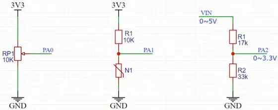
Figure 7: Circuit Examples
The two fixed ends of the potentiometer, one end is connected to 3.3V, and the other end is connected to GND, so that the sliding end in the middle can output an adjustable voltage of 0~3.3V. Here you can connect the input channel of the ADC such as PA0 port. When slides up, the voltage increases, and when slides down, the voltage decreases. The resistance of the resistor should not be too small, because it is directly connected to the positive and negative poles of the power supply. Generally, a K-ohm resistor should be connected.
In the middle is the sensor circuit for the output voltage. In general, photoresistors, thermistors, infrared receiving tubes, and microphones can all be equivalent to a variable resistor. The resistance value cannot be directly measured. It can be connected in series with a fixed resistor to get a circuit that responds to the resistance value. Where the sensor resistance becomes smaller, the pull-down effect becomes stronger, and the output terminal voltage drops; when the sensor resistance value becomes larger, the pull-down effect becomes weaker, and the output terminal is affected by the pull-up resistor. The voltage will rise. The fixed resistor generally chooses the capacitor, whose capacitance close to the resistance of the sensor.
The circuit on the right is a simple voltage conversion circuit. If you want to measure a VIN voltage of 5V but the ADC can only receive a voltage of 3.3V, then a simple conversion circuit can be used. Employ a resistor to divide the voltage, and the upper resistance is 17K. The lower is 33K, and the intermediate voltage is 3.3V. Finally it can enter the ADC conversion, which is a simple voltage conversion circuit.
ADC Initialization Steps
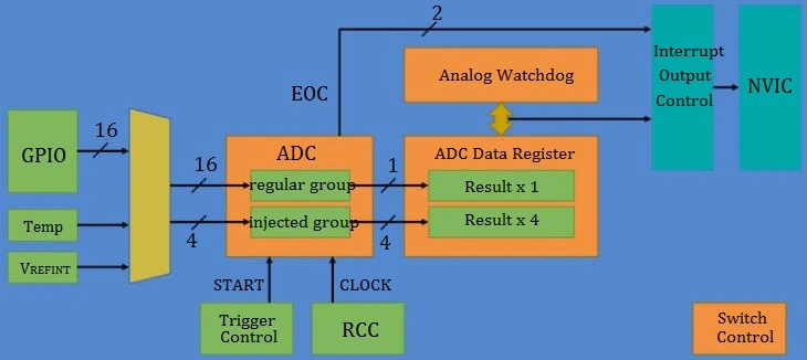
Fgiure 8: Basic ADC Structure
Step 1: Turn on the RCC clock, including the clock of ADC and GPIO, and the frequency divider of ADCCLK also needs to be configured
Step 2: Configure GPIO as an analog input mode
Step 3: Configure the multi-way switch and connect the channel on the left to the regular group list on the right.
Step 4: Configure the ADC converter, using the library function to configure the parameters of the large circuit.
Step 5: Call ADC_Cmd to turn on the ADC, and you can also perform a calibration to reduce the error.
After completing these steps, there will be a function to trigger operations and read the results.
ADC Related Functions
ADCCLK Configuration Functions
The 72MHz clock of APB2 can be divided by 2, 4, 6, and 8, and then input to ADCCLK.
void RCC_ADCCLKConfig(uint32_t RCC_PCLK2)
Restore default configuration function.
void ADC_DeInit(ADC_TypeDef* ADCx);
Init function
void ADC_Init(ADC_TypeDef* ADCx, ADC_InitTypeDef* ADC_InitStruct);
StructInit function
void ADC_StructInit(ADC_InitTypeDef* ADC_InitStruct);
Function to power up the ADC
void ADC_Cmd(ADC_TypeDef* ADCx, FunctionalState NewState);
Turn on the DMA output signal function and call it when data needs to be transferred.
void ADC_DMACmd(ADC_TypeDef* ADCx, FunctionalState NewState);
Interrupt output control function
void ADC_ITConfig(ADC_TypeDef* ADCx, uint16_t ADC_IT, FunctionalState NewState);
Reset calibration function
void ADC_ResetCalibration(ADC_TypeDef* ADCx);
Get reset calibration status function
FlagStatus ADC_GetResetCalibrationStatus(ADC_TypeDef* ADCx);
Start Calibration function
void ADC_StartCalibration(ADC_TypeDef* ADCx);
Get Start Calibration Status function
FlagStatus ADC_GetCalibrationStatus(ADC_TypeDef* ADCx);
Software trigger ADC function
void ADC_SoftwareStartConvCmd(ADC_TypeDef* ADCx, FunctionalState NewState);
ADC acquisition software start conversion-state function
Get the SWSTART bit of CR2 and set SWTART to 1 to start the conversion. This function returns the status of SWSTART. Since the SWSTART bit is cleared to 0 immediately after the conversion starts, the return value of this function has nothing to do with the conversion.
FlagStatus ADC_GetSoftwareStartConvStatus(ADC_TypeDef* ADCx);
A function use to get whether the conversion is finished.
Obtain the status of the flag bit, give the parameter to the flag bit of EOC, and judge whether the EOC flag bit is set to 1. If the conversion ends and the EOC flag bit is set to 1, then use this function to judge the flag bit, that is, judge whether the conversion is over.
FlagStatus ADC_GetFlagStatus(ADC_TypeDef* ADCx, uint8_t ADC_FLAG);
Configure intermittent mode functions
void ADC_DiscModeChannelCountConfig(ADC_TypeDef* ADCx, uint8_t Number);// interrupt every few channels
void ADC_DiscModeCmd(ADC_TypeDef* ADCx, FunctionalState NewState);// enable intermittent mode
Channel configuration function of ADC regular group, which is to fill in the specified channel for each position of the sequence.
void ADC_RegularChannelConfig(ADC_TypeDef* ADCx, uint8_t ADC_Channel, uint8_t Rank, uint8_t ADC_SampleTime);
External trigger conversion control function, whether to allow external trigger conversion
void ADC_ExternalTrigConvCmd(ADC_TypeDef* ADCx, FunctionalState NewState);
ADC get conversion value function, which is used to read conversion structure.
uint16_t ADC_GetConversionValue(ADC_TypeDef* ADCx);
The function is to obtain the conversion value of dual mode for ADC.
uint32_t ADC_GetDualModeConversionValue(void);
Injected group related functions
void ADC_AutoInjectedConvCmd(ADC_TypeDef* ADCx, FunctionalState NewState);
void ADC_InjectedDiscModeCmd(ADC_TypeDef* ADCx, FunctionalState NewState);
void ADC_ExternalTrigInjectedConvConfig(ADC_TypeDef* ADCx, uint32_t ADC_ExternalTrigInjecConv);
void ADC_ExternalTrigInjectedConvCmd(ADC_TypeDef* ADCx, FunctionalState NewState);
void ADC_SoftwareStartInjectedConvCmd(ADC_TypeDef* ADCx, FunctionalState NewState);
FlagStatus ADC_GetSoftwareStartInjectedConvCmdStatus(ADC_TypeDef* ADCx);
void ADC_InjectedChannelConfig(ADC_TypeDef* ADCx, uint8_t ADC_Channel, uint8_t Rank, uint8_t ADC_SampleTime);
void ADC_InjectedSequencerLengthConfig(ADC_TypeDef* ADCx, uint8_t Length);
void ADC_SetInjectedOffset(ADC_TypeDef* ADCx, uint8_t ADC_InjectedChannel, uint16_t Offset);
uint16_t ADC_GetInjectedConversionValue(ADC_TypeDef* ADCx, uint8_t ADC_InjectedChannel);
Configure Analog Watchdog Related Functions
void ADC_AnalogWatchdogCmd(ADC_TypeDef* ADCx, uint32_t ADC_AnalogWatchdog);// whether to start the analog watchdog
void ADC_AnalogWatchdogThresholdsConfig(ADC_TypeDef* ADCx, uint16_t HighThreshold, uint16_t LowThreshold);// configure high and low thresholds
void ADC_AnalogWatchdogSingleChannelConfig(ADC_TypeDef* ADCx, uint8_t ADC_Channel);// configure the gatekeeper channel
In order to control ADC temperature sensor and internal reference voltage control), you can employ this function.
void ADC_TempSensorVrefintCmd(FunctionalState NewState);
Get flag status function
FlagStatus ADC_GetFlagStatus(ADC_TypeDef* ADCx, uint8_t ADC_FLAG);
Clear flag function
void ADC_ClearFlag(ADC_TypeDef* ADCx, uint8_t ADC_FLAG);
Get interrupt status function
ITStatus ADC_GetITStatus(ADC_TypeDef* ADCx, uint16_t ADC_IT);
Clear interrupt pending bit
void ADC_ClearITPendingBit(ADC_TypeDef* ADCx, uint16_t ADC_IT);
ADC Program Example
void AD_Init(void)
{
RCC_APB2PeriphClockCmd(RCC_APB2Periph_ADC1, ENABLE);
RCC_APB2PeriphClockCmd(RCC_APB2Periph_GPIOA, ENABLE);
RCC_ADCCLKConfig(RCC_PCLK2_Div6);
GPIO_InitTypeDef GPIO_InitStructure;
GPIO_InitStructure.GPIO_Mode = GPIO_Mode_AIN;
GPIO_InitStructure.GPIO_Pin = GPIO_Pin_0 | GPIO_Pin_1 | GPIO_Pin_2 | GPIO_Pin_3;
GPIO_InitStructure.GPIO_Speed = GPIO_Speed_50MHz;
GPIO_Init(GPIOA, &GPIO_InitStructure);
ADC_InitTypeDef ADC_InitStructure;
ADC_InitStructure.ADC_Mode = ADC_Mode_Independent;// independent mode
ADC_InitStructure.ADC_DataAlign = ADC_DataAlign_Right;// right align
ADC_InitStructure.ADC_ExternalTrigConv = ADC_ExternalTrigConv_None;// software trigger
ADC_InitStructure.ADC_ContinuousConvMode = DISABLE;// continuous mode
ADC_InitStructure.ADC_ScanConvMode = DISABLE;// scan mode
ADC_InitStructure.ADC_NbrOfChannel = 1;// number of channels
ADC_Init(ADC1, &ADC_InitStructure);
ADC_Cmd(ADC1, ENABLE);// enable ADC
ADC_ResetCalibration(ADC1);// start reset calibration
while (ADC_GetResetCalibrationStatus(ADC1) == SET);// get reset calibration status
ADC_StartCalibration(ADC1);// start calibration status
while (ADC_GetCalibrationStatus(ADC1) == SET);// get calibration status
}
uint16_t AD_GetValue(uint8_t ADC_Channel)
{
ADC_RegularChannelConfig(ADC1, ADC_Channel, 1, ADC_SampleTime_55Cycles5);// functions to set regular groups
ADC_SoftwareStartConvCmd(ADC1, ENABLE);// software trigger
while (ADC_GetFlagStatus(ADC1, ADC_FLAG_EOC) == RESET);// get the calibration complete flag
return ADC_GetConversionValue(ADC1);// return the converted AD value
}

 English










