Wafer Basics
Wafer Size
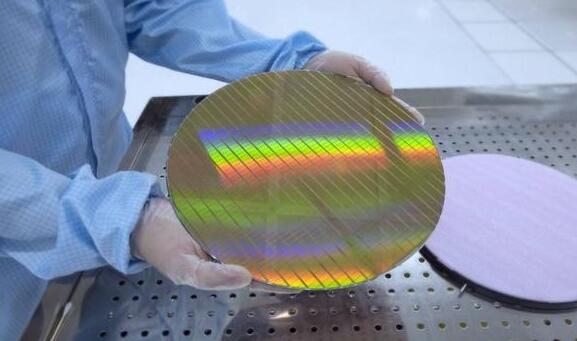
In chip production, what do we often refer to as 300mm/450mm, 8-inch/12-inch wafers? In fact, it is easy to understand that this number expresses the size or diameter of the wafer literally, while millimeters and inches are just different units of measurement. What’s more, the larger the size or diameter, the larger the wafer and the greater the number of chips produced.
* Wafer Size Lists
|
Wafer Size
|
Year Introduced
|
|
1-inch (25 mm)
|
1960
|
|
2-inch (51 mm)
|
1969
|
|
3-inch (76 mm)
|
1972
|
|
4-inch (100 mm)
|
1976
|
|
4.9-inch (125 mm)
|
1981
|
|
5.9-inch (150 mm), usually known as the "6-inch"
|
1983
|
|
7.9-inch (200 mm), usually known as the "8-inch"
|
1992
|
|
11.8-inch (300 mm), usually known as the "12-inch"
|
2002
|
|
17.7-inch (450 mm)
|
2020
|
|
26.6-inch (675 mm)
|
-
|
Wafer Applications
The diameters of wafers currently on the market are mainly 150mm, 200mm, and 300mm, corresponding to 6-inch, 8-inch, and 12-inch wafers respectively. The mainstream are 200mm and 300mm, which are 8-inch, 12-inch wafers, accounting for all about 80% of the wafer market.
8-inch Wafers
• For 8-inch wafers, IC usage (arranged by price from high to low)
• Metal Oxide Semiconductor Field Effect Transistors (MOSFETs): 110-300 nm
• LED driver IC: 300–500 nm
• NOR Flash IC: 100-180 nm
• Audio IC: 110-300nm
• DDIC: 110-300nm, especially for large-size TFT LCD panels of 9 inches and above
• T-cons: 110-180nm
• CIS: 110–280 nm
• TPM ICs: 110–280 nm
• PMICs: 110–280 nm
• Retimer/redriver IC (for PC internal transmission): 110-180 nm
• USB Controller: 110-180 nm
• MCUs, especially for automotive applications: 150-300 nm
MCU is the most expensive chip using 8-inch wafer, while DDIC is in the middle. On the one hand, when MCU demand surges, 8-inch wafers tend to produce more MCUs than lower-priced MOSFETs. On the other hand, the demand for PMIC and DDIC is stable, so foundry manufacturers always allocate a certain capacity for PMIC and DDIC. However, the growth of electric vehicles, 5G telecommunications, and less power consumption issues in all devices have led to a surge in demand for PMICs, which affects the capacity allocation of them by wafer foundries.
12-inch Wafers
• For 12-inch wafers, IC usage (arranged by price from high to low)
• NOR Flash ICs: 55–90 nm
• T-cons: 22–90 nm
• DDIC for Smartphone LCD and OLED: 28-55nm
• CIS: 22–90 nm
• TPM IC: 40–60 nm
• PMIC: 55–90 nm
• Retimer/redriver IC (for PC internal transmission): 110-180 nm
• USB controllers: 28–90nm
• MCU: 40–90nm
• Memory control IC: 28–40nm
• Complex Programmable Logic Devices (CPLDs), also logic ICs: 22-28 nm
• Field Programmable Gate Array (FPGA), usually custom: 22-28 nm
• BMCs for PC servers and networking equipment: 28-60 nm
• Network ICs: Sub-14 nm and 14-55 nm, depending on design and specification
• CPU, including GPU: below 14 nm
In 12-inch fabs, CPU and GPU are the most profitable products. Foundry manufacturers are concerned about the profitability of fabs, not maintaining 100% capacity utilization. In terms of IC prices, DDIC is one of the lowest-priced products in 12-inch wafer products. The increase in demand for OLED and notebook display panels has seized more production capacity of the 40-55 nm process in 12-inch fabs.
Wafer Defects and Their Causes
1) Surface Redundancy
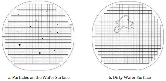
There are many types of redundancy on the wafer surface, ranging from tiny particles as small as tens of nanometers, to dust as large as hundreds of microns, and surface residues left by the previous process. On the one hand, during processes such as etching, polishing, cleaning, etc. may cause particles. On the other hand, their are dust on the air and chemical reagents during processing. The particles will block the light during photolithography, causing defects in the structure of the integrated circuit. And contaminants may adhere to the surface of the wafer, resulting in incomplete patterns and affecting the electrical characteristics of the chip.
2) Crystal Defect
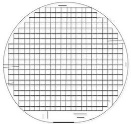
Slip line defect is also a common problem, which is caused by uneven heating during crystal growth. They are thin horizontal straight lines at the peripheral edge of the wafer. Due to the relatively large size of the slip line, it can be identified by manual.
Stacking fault is also a defect that can be found in the epitaxial layer. It is generally due to the destruction of the normal stacking order of the close-packed planes in the crystal structure, and its size is usually at the micron level.
3) Mechanical Injury
Mechanical damage generally refers to the scratches on the surface of the wafer caused by polishing or slicing, usually caused by chemical mechanical polishing (CMP), in an arc shape, or in a discontinuous point distribution. This kind of damage varies in size and usually affects the connectivity of the wafer circuit, which is a relatively serious. However, it can be corrected, sometimes improper operation of the machine can be avoided to the most extent.
4) Wafer Cleaning
• It refers to the process of removing pollutants and oxides on the wafer surface by chemical or physical methods during the manufacturing process of integrated circuits, so that the surface of the wafer meets the cleanliness requirements. The principle of wafer cleaning is to remove various impurities without damaging the wafer.
• There are four main methods for the removal of particles: dissolution, oxidative decomposition, electrical repulsion between particles and the surface of the silicon wafer, and very slight corrosion on the surface of the silicon wafer.
• For the removal of metal particles, SC-2 solution or HPM solution is usually used to reduce the metal content on the wafer surface. The SC-2 solution will crystallize, which may increase the number of particles on the wafer surface after cleaning. Therefore, HCL can be replaced by HF, or SC-2 solution can be replaced by O3 and HF, which can also remove metal particles well.
• For organic pollutants, SPM solution or UV/ozone dry cleaning technology is usually used to remove them.
• The wafers after wet cleaning must be thoroughly dried to ensure that there are no sign on the surface before they can enter the next step of the process. The three most common drying modes at present are spin drying, marangoni drying and hot isopropanol atomizing drying.
8-inch Wafer Shortage Factors
• First, in terms of long-term demand, automobiles, industries, and smartphones are the main applications of 8-inch wafers. The development of 5G, electric vehicles, intelligent manufacturing, and the Internet of Things (IoT) has led to strong demand for non-advanced chips in areas such as FPGA, driver chips, fingerprint recognition, power management, mosfets, and microcontrollers (MCU).
• Second, since the first half of 2020, COVID-19 has affected wafer production capacity and logistics largely.
• Third, the global home office and online education have led to a significant increase in shipments of notebook computers and tablet products, driving demand for display driver ICs and power management ICs for medium and large-sized panels.
• Fourth, in the second half of 2020, the COVID-19 has been initially controlled, for the automobile market, especially the new-energy vehicle market, has gradually recovered, and the consumption of IGBTs and MOSFETs has increased significantly, both of which have brought new growth in 8-inch wafer manufacturing. The backlog of unfinished orders affected by the epidemic has continued to the second half of the year, resulting in insufficient supply, so the momentum of price increases is gradually transmitted from upstream to downstream.
• Fifth, the U.S. ban has prompted major Chinese electronics manufacturers, including Huawei, OPPO, Vivo, and Xiaomi, to stock up, further occupying production capacity.
In the case of a surge in order demand and limited production capacity, 8-inch wafer foundries have begun to screen new orders and adjust product set, giving priority to the production of products with high gross profit margins, while products with low-gross profit margins are relatively weak in market preemption. And chip production capacity is tilted towards large customers, and small manufacturers face greater pressure to compete for production capacity.
Affected by production capacity, the delivery time of major chip manufacturers are far outside the standard time, so the chips shortage caused by the backlog of orders will continue. Here is the delivery time of the big semiconductor manufacturers:
|
Semiconductor Manufacturers
|
Delivery Time
|
|
STMicroelectronics
|
20~26 weeks, including automotive chips
|
|
NXP
|
Standard is 16~20 weeks, actually more than 26 weeks
|
|
Renesas
|
20~24 weeks
|
|
Texas Instruments
|
Average is 30 weeks, individual around 50 weeks
|
|
Toshiba
|
24 weeks
|
|
Qualcomm
|
The whole series is more than 30 weeks, and the CSR Bluetooth chip needs more than 33 weeks
|
|
Broadcom
|
Around 50 weeks
|
|
Altera
|
Standard is 6~8 weeks
|
|
Maxim
|
Standard is 8~10 weeks, extended to 20 weeks
|
|
Murata
|
Minimum is 16 weeks, maximum is 26 weeks
|
|
Silicone
|
At least 14 weeks
|
Does Wafer Size Matter?
In theory, a larger wafer diameter enables producing more semiconductor devices from a single wafer. That is, the bigger the wafer, the more stuff it can hold, which improves the manufacturing productivity and efficiency, thus making electron devices more powerful. Actually, bigger is not always better.
Wafer is silicon slice which obtained by cutting single crystal silicon rods. The Czochralski method is generally used to get silicon rods. The slower the rotation speed during the crystallization process, the larger the diameter, but the larger the diameter and unstable rotation speed may lead to wafer structure defect. At the same time, the larger the diameter means the heavier the wafer, and the wafer edge will be more likely warp. Therefore, the larger the wafer, the lower the yield and the higher the cost. Generally speaking, the purpose of increasing the wafer diameter is to increase the utilization rate of single-crystal silicon and reduce the cost. When the reduced cost cannot make up for the increased cost in the production of large-diameter wafers, it becomes unnecessary to choose larger-sized wafers for production. In addition, the equipment for producing wafers is expensive, and the cost of upgrading the entire production line is very high. The conclusion is that the increased benefit cannot offset the cost increase caused by various factors, so the larger wafer is not always good. Electronics use wafer sizes from 100 to 450 mm diameter, even the largest wafers made have a diameter of 675 mm, but are not yet in general use.
Biggest Semiconductor Foundries in 2023
1) Taiwan Semiconductor Manufacturing Co. Ltd. (TSMC)
TSMC is the world's largest semiconductor foundry. The annual capacity of the manufacturing facilities and its subsidiaries exceeded 12 million 12-inch equivalent wafers in 2020. These facilities include four 12-inch wafer GIGAFAB® fabs, four 8-inch wafer fabs, and one 6-inch wafer fab – all in Taiwan – as well as one 12-inch wafer fab at a wholly owned subsidiary, TSMC Nanjing Company Limited, and two 8-inch wafer fabs at wholly owned subsidiaries, WaferTech in the United States and TSMC China Company Limited.
2) Samsung Electronics
Samsung Electronics is offering competitive processes, design technologies, IP, and high-volume manufacturing capability for customers. The full suite of advanced process technologies includes 28FD-SOI, 14/10/8/5/4nm FinFet, and 3nm GAA with EUV technology from 5nm. For the application-specific technologies, RF, eNVM, high voltage, BCD, CMOS image sensors and finger print sensors are offered. In concert with its process technology leadership, Samsung Foundry provides integrated package solutions including 3D/2.5D. Samsung Foundry’s SAFE program also offers a full range of verified EDA/DM solutions, product-proven IPs, a flexible design environment through cloud, and a comprehensive ASIC design service.
3) GlobalFoundries (GF)
GlobalFoundries Inc. (GF or GloFo) is a multinational semiconductor contract manufacturing and design company. GF manufactures integrated circuits on wafers designed for markets such as mobility, automotive, computing and wired connectivity, consumer internet of things (IoT) and other industrial applications.It is the only one with operations in Singapore, the European Union, and the United States: one 200 mm and one 300 mm wafer fabrication plant in Singapore; one 300 mm plant in Dresden, Germany; one 200 mm plant in Burlington, Vermont and two 300 mm plants in the State of New York: one in East Fishkill and one in Malta.
4) United Microelectronics Corporation (UMC)
United Microelectronics Corporation is a Taiwanese company based in Hsinchu, Taiwan.UMC has 12 wafer fabs located throughout Asia, including four advanced 12-inch fabs. Fab 12A in Tainan, Taiwan has been in volume production for customer products since 2002 and is currently manufacturing products down to 14nm. UMC's second 12-inch fab, Fab 12i, is located in Singapore. This facility is the company’s specialty technology center that provides highly specialized processes on 12-inch manufacturing to serve a diverse range of product applications. United Semi, located in Xiamen, China, was established as southern China's first 12-inch foundry fab and began volume production in 2016. United Semi serves China's vast IC market and provides high quality, geographically diversified manufacturing for our foundry customers. Japan-based USJC, fully acquired in October of 2019, is UMC’s fourth 12-inch fab. USJC offers foundry volume production for mature specialty nodes ranging from 90-nanometer to 40-nanometer.
5) Semiconductor Manufacturing International Corporation (SMIC)
Semiconductor Manufacturing International Corporation is a partially state-owned publicly listed Chinese pure-play semiconductor foundry company.SMIC Group provides semiconductor foundry and technology services to global customers on 0.35 micron to FinFET process node technologies. Headquartered in Shanghai, China, SMIC has an international manufacturing and service base, with three 8-inch wafer fabrication facilities (fabs) and four 12-inch fabs in Shanghai, Beijing, Tianjin and Shenzhen, and three 12-inch fabs under construction in Shanghai, Beijing and Tianjin.

 English