FinFET is a kind of “3D transistors” that has lower leakage and greater device density. It is similar to that of a general MOSFET, but it is nonplanar and multi-gate. So what is the relationship between FinFET and MOSFET? and how it was formed?
FinFET Key Points Introduction
Short Brief
Fin field-effect transistor, also called FinFET, is an innovative design of the traditional standard field-effect transistors, that is, a new complementary metal oxide semiconductor transistor. In the traditional transistor structure, the gate that controls the passage of current can only control the on and off of the circuit on one side, which belongs to the planar structure. In the FinFET structure, the gate is formed into a fork-shaped 3D structure similar to a fish fin, which can control the on and off of the circuit on both sides of the circuit. This design can greatly improve circuit control and reduce leakage, and can also greatly shorten the gate length of the transistor.
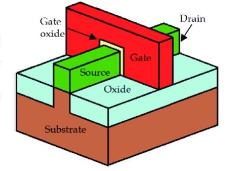
Figure 1: FinFET Structure Diagram
FinFET is a linking technology in the semiconductor process. When talking about FinFET, we have to mention planar MOSFET.
MOSFET Structure
The metal–oxide–semiconductor field-effect transistor (MOSFET), as shown in the figure below, this structure and its working principle have been introduced in many articles, which consists of three electrodes: gate G, drain G and source S.
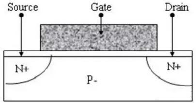
Figure 2: MOSFET Basic Structure
The working principle of the MOSFET is very simple. Electrons flow in from the left Source, pass through the electron channel under the Gate, and flow out from the right Drain. The middle gate can decide whether to let the electrons pass through; electrons flow in from the source, which is the source of electrons, so it is called a "source"; and electrons flow out from the drain.
MOSFET can be divided into NPN-type and PNP-type. The NPN type is usually called the N-channel type, and the PNP type is usually called the P-channel type. For an N-channel field effect transistor, its source and drain are connected to an N-type semiconductor, and for a P-channel field effect transistor, its source and drain are connected to a P-type semiconductor. We know that a general triode controls the output current by the input current. But for field effect tubes, its output current is controlled by the input voltage (or field voltage), and it can be considered that the input current is very small or there is no input current.
Taking the planar enhancement type N-channel MOSFET as an example, the basic structure is shown in the figure below. It can be seen that the doping of NPN from left to right will naturally form a deep red depletion region under the action of diffusion. According to the previous description, the depletion region is non-conductive. Therefore, the drain to the source is disconnected when no external electric field is applied, so the structure is a normal-off structure.
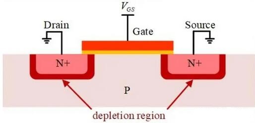
Figure 3: Enhanced N-channel MOSFET
Note that the central area in the figure is the core part mentioned earlier. From top to bottom, orange, yellow, and light red are metal, oxide, and P-doped. When Vgs>0, a new depletion layer will start to form under the oxide layer first, as shown below.
When Vgs>Vth (threshold voltage), an inversion layer (described below) is formed, as shown in the figure below. Since the inversion layer is equivalent to an N-doped semiconductor, D and S are directly connected, so the conduction channel is formed.
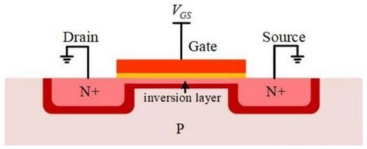
Figure 4: MOSFET Inversion Layer
Let's talk about the inversion layer and threshold voltage.
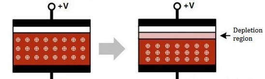
Figure 5: Depletion Region
The red area is P-doped. There are holes (positive charges) in the red area, which will go down away under the action of the external electric field, thus forming a region without free carriers on the upper surface, namely the depletion region. When the applied voltage is high enough, the holes in the depletion layer will be further driven away, and electrons will be attracted to move to the upper surface, and electrons that can conduct electricity will be accumulated on the upper surface to form an N-type semiconductor, thereby forming an inversion layer (the free carriers in this region are opposite to the semiconductor carriers formed by doping). Generally, we call the voltage applied when the inversion layer starts to form as Vth, which is the threshold voltage. The inversion layer is also the conductive channel (formed in the horizontal direction).
The width of the Gate, that is, the trench width or line width (usually referred to as the um of the CPU process), and the number of nm refers to this width, not the size of each unit cell.
The reduction of the width of the trench GATE can bring the following advantages:
(1) The groove width corresponds to the distance from D to S. When it is reduced, the conduction time of carrier flow across the channel is reduced, so that the switching frequency allowed to work can be increased.
(2) The trench width is small, the G electrode voltage applied when the channel is fully opened can be reduced, the conduction is easier, and the switching loss is reduced.
(3) The trench width is reduced, the on-resistance of the channel is reduced, and the conduction loss is further reduced.
Because of these advantages, semiconductor manufacturing companies are also driven to continuously adopt new processes and pursue lower process sizes to improve the performance of semiconductor devices and reduce power consumption.
FinFET Generation Background
Look at the following typical MOS structure. In the previous process evolution, such as 0.35um, 0.18um, 90nm, 65nm, etc., the gate width in the middle was narrowed, which is the core technology of process evolution. These numbers actually refer to the width of the gate in the lateral direction.
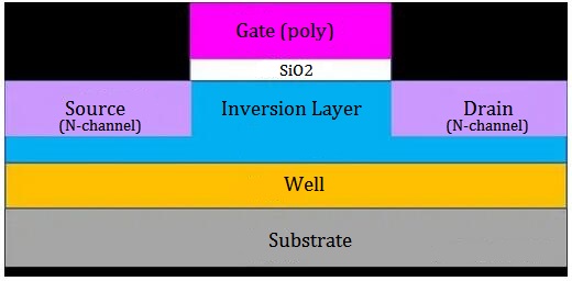
Figure 6: MOSFET Architecture
However, when the traditional MOS structure was developed to around 22nm, there appeared two problems that every semiconductor person did not want to meet.
(1) If the line width is further reduced according to the original MOS structure, the source and drain terminals will be easily short-circuited. It is very easy for electrons to "accidentally" run from the source to the drain, which is not controlled by the gate. This is very undesirable because it will cause the circuit to fail.
(2) The saturation current is too small, in other words, the current from the source to the drain is too small. Of course, we hope that the larger the current, the better, because the larger the difference between the MOS on state and the off state, called good switching characteristics.
So what to do? So people invented FinFET and SOI technology to solve this problem. Since FinFET is now the mainstream technology, TSMC, Intel, Samsung, and SMIC all use it. While SOI technology is only used by GF now, so we mainly talk about FinFET technology.
FinFET Principle
In 1998, Professor Hu Zhengming of the UC Berkeley further proposed a self-aligned double-gate MOSFET structure based on the three-dimensional structure of the MOS transistor and the double-gate MOSFET structure. Because the shape of the transistor is similar to a fish fin, it is called FinFET. In the same year, Professor Hu and his team members successfully manufactured the first n-type FinFET with a gate length of only 17nm, a channel width of 20nm, and a fin height of 50nm. In 1999, they successfully made the first p-type FinFET with a gate length of only 18nm, a channel width of 15nm, and a fin height of 50nm. FinFET was born since then.
As for the FinFET architecture, the gate is designed as a fork-shaped 3D structure, which can control the on and off of the circuit on both sides of the circuit, and increases the surface of the gate around the channel, strengthens the control of the gate on the channel, not only improves circuit control and reduces leakage current, but also greatly reduces the gate length of the transistor. In the process evolution of Metal gate, poly gate is replaced by metal gate. SiO2 is also replaced by high-K.
In 2011, Intel used the FinFET process on its third-generation Core processor, and then major semiconductor manufacturers also began to switch to the FinFET process, including TSMC’s 16nm &10nm, Samsung’s 14nm & 10nm and GlobalFoundries’s 14nm. However, the limit of the FinFET process is the 7nm process, then it will need to rely on extreme ultraviolet lithography.
Nanoprocess of Top Semiconductor Manufacturers
We often encounter a problem, such as TSMC’s 14nm mass production and Samsung’s 7nm mass production. So how are 7nm and 14nm defined here? Let me talk about one thing first, Intel uses FinFET technology at 20nm/22nm, Samsung and TSMC use FinFET technology at 16nm and 14nm. However, they used the planar structure before.
In fact, after using FinFET, the number of nanometers does not refer to the width of the gate, neither the width of the fin. For example, in the 7nm process, none of the structures are 7nm. These numbers are just a virtual number. It is named after the law of Moore's Law. Assuming that at 22nm, only 100 transistors can be accommodated in 1 square micron, according to Moore's law, when it is manufactured at 14nm/16nm, 1 square micron should be able to accommodate 200 transistors. Therefore, no matter how wide the fin is, as long as this condition is met, it can be called a 14nm process. Below we briefly list the main parameters related to pattern density of Intel, Samsung, TSMC and so on.
|
|
Intel
|
TSMC
|
Samsung
|
Intel
|
|
Process Name
|
22nm HP
|
16nm FF+
|
14nm FF+
|
14nm HP
|
|
Supply Voltage (V)
|
0.75
|
0.75
|
0.8
|
0.7
|
|
Minimum Gate Length (nm)
|
2
|
30
|
20
|
20
|
|
Contacted Gate Metal (nm)
|
90
|
90
|
78
|
70
|
|
Minimum Metal Pitch (nm)
|
80
|
64
|
64
|
52
|
|
HD SRAM Cell Size (um2)
|
0.092
|
0.070
|
0.064
|
0.050
|
|
Apple A9 Die Size (mm2)
|
Not applicable
|
104.5
|
96
|
Not applicable
|
|
Volume Production
|
2Q12
|
3Q15
|
1Q15
|
4Q14
|
|
|
|
Feature
|
Intel
|
TSMC
|
Samsung
|
Intel transistors are smaller than TSMC or Samsung
|
|
Gate length (nm)
|
24
|
33
|
30
|
|
Min contacted gate pitch (nm)
|
70
|
90
|
78
|
|
Fin height under gate (nm)
|
42
|
37
|
37
|
|
Fin pitch (nm)
|
43
|
45
|
49
|
|
Min metal pitch (nm)
|
52
|
70
|
67
|
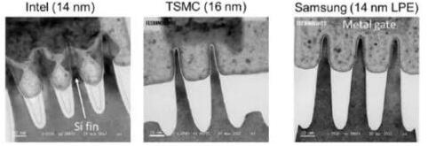
It can be seen that according to the slicing pieces, regardless of the parameters such as gate length, fin pitch, and metal pitch, Intel is smaller than Samsung and TSMC under the same process. So now many people say that Intel's 14nm is TSMC Samsung's 10nm, and Intel's 10nm is TSMC Samsung's 7nm.
GAAFET Is Coming
With the further shrinking of the chip manufacturing process, such as 5nm, 3nm, and 2nm, FinFET also has its limits: too close distance between fins, leakage, and physical materials limits Also, as the process shrinks, if three fins can be placed on a FinFET transistor, now only one can be placed, so the fins have to be heightened. But a new problem appeared. After reaching a certain height, it is difficult to keep upright under the action of internal stress, which is not the FinFET structure any longer.
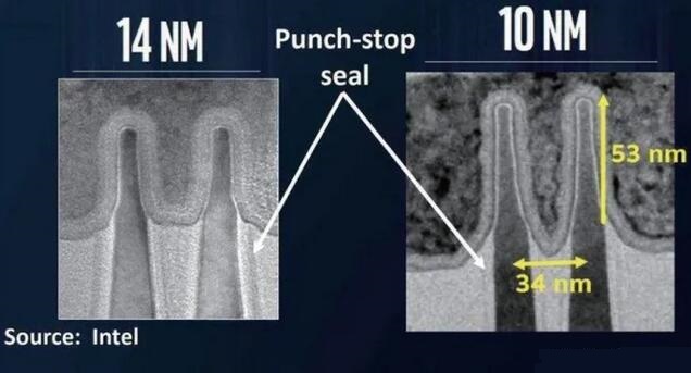
Figure 7: 3D FinFET
In short, after 5nm, FinFET can no longer be used. At this time, it is the turn of GAAFET technology. The full name of GAA is Gate-All-Around, which means GAAFET is a wrap-around gate transistor. In 1990, Dr. Cor Claeys of Belgium IMEC and his research team proposed it in an article. In fact, GAAFET is equivalent to an improved version of FinFET. The transistor structure under this technology has changed again. The gate and drain are no longer fins, but become sticks that pass through the gate vertically. In this way, the gate can realize four-sided wrapping of the source and drain. It looks like the source and drain were fins, and now the gates are fins. So GAAFET and FinFET have many similarities in principle.
In any case, from the three-contact surface to the four-contact surface, and it has been split into several four-contact surfaces, it is obvious that this time the gate's control over the current has been further improved. In addition, this design of GAAFET can also solve the original problem of shrinking the pitch of the fins, and to a large extent solve the problems caused by the shrinking of the gate pitch, such as capacitive effects.

Figure 8: FinFET vs GAA(MBCFET)
In short, with the innovation of GAAFET technology, the evolution of semiconductor process will go further, and it will become a keyword that everyone often hears after 5nm with better device performance than FinFET. If you want to know more about electronics info, just mark our web KUKE.

 English










