Semiconductor materials are key components in modern electronics, serving as the foundation for devices like transistors, diodes, solar cells, and integrated circuits. They are materials that have electrical properties between conductors (such as metals) and insulators (such as ceramics). Their ability to conduct electricity can be precisely controlled by introducing impurities (doping), making them highly versatile for a variety of applications. What are they? Look at this article you can get the key points.
Raw Materials
1. Silicon Wafers & Substrates
Silicon wafers are thin slices of high-purity crystalline silicon. They are used as the substrate of chips and are found in almost every electronic device. Silicon is the second most common element on earth, which is common in sand and quartz. And Si is one of the main elements in building materials such as bricks, cement and glass.
Silicon is currently the most widely used material in semiconductor industry. Although silicon chips may look like metal, they are not exactly metal. In addition, a pure silicon crystal is almost an insulator; very little current is allowed to pass through it. However, doped silicon wafers can change its conductivity.
Doping is mixing small amounts of impurities into a silicon crystal to change its behavior and integrate it into a conductor. These impurities used for doping are called dopants. Silicon itself does not conduct electricity well; however, it can be precisely doped to control resistivity to precise levels. Silicon dopants such as nitrogen, indium, aluminum, gallium and boron are added during chip manufacturing. Therefore, for non-conductive silicon to form a semiconductor, the silicon must be turned into a wafer. Silicon wafers come in many shapes and sizes, depending on their purpose. Wafers range from 2 inches to 12 inches, with 6 inches, 8 inches and 12 inches being the most common ones. They are key materials in integrated circuits.
2. Compound Semiconductors
Compound semiconductors mainly refer to second- and third-generation semiconductors such as gallium arsenide (GaAs), gallium nitride (GaN), and silicon carbide (SiC). Compared with the first-gen elemental semiconductors, they are much better in high-frequency and high-temperature performances.
GaAs: It has the characteristics of high frequency, radiation resistance, and high temperature resistance. Widely used in the field of wireless communications and has now become the mainstream material for PA and Switch.
GaN: It is mainly used in communication base stations, power devices and other fields. The power amplifier has high efficiency and high power density, so it can save a lot of power and reduce the size and quality of the base station.
SiC: Mainly used for high-power and high-frequency power devices. IHS predicts that the market size of SiC power semiconductors is expected to reach US$3 billion by 2025. In the next 10 years, SiC devices will begin to be widely used in industry and electric vehicles. As the industrialization of it begins to accelerate, world famous manufacturers such as STMicroelectronics and Infineon begin to lock in upstream wafer supplies.
Table 1: Different Compound Semiconductors Application Fields
|
Industries
|
Components
|
Materials
|
Application Fields
|
|
Optoelectronics
|
Optoelectronic ICs, laser diodes, photodetectors, photovoltaic devices, etc.
|
GaAs, InP, GaN
|
Optical fiber communications, optical wireless communications, data centers, general lighting, displays, photovoltaic cells, etc.
|
|
Radio Frequency Communications
|
Power amplifiers, RF switches, LNAs, filters, mixers, microwave integrated circuits, etc.
|
GaAs, InP, GaN
|
Mobile communication equipment and bases, radar, WiFi/Bluetooth modules, satellite communications, CATV, etc.
|
|
Power Electronics
|
Schottky diode (SBD), MOSFET, IGBT
|
GaN, SiC, Si
|
Household appliances, new energy vehicles, UPS, photovoltaic/wind energy power stations, smart grids, high-speed trains, etc.
|
|
Quantum High-end ICs
|
*
|
GaAs, InP, etc.
|
High-performance computers, servers, photonic computers, quantum computers, etc.
|
Manufacturing Materials
1. Mask
An integrated circuit (IC) is manufactured in part using photomasks (Mask). According to the pattern required by the customer, a photolithography machine is used to etch the corresponding pattern on the raw material, and the unnecessary metal layer and adhesive layer are washed away to obtain the mask. Mask is a graphic master used in the photolithography process in microelectronic. It consists of an opaque light-shielding film forming a mask on a transparent substrate, and transfer the graphics to the product substrate through exposure. In short, it is used to transfer high-precision circuit designs and carries intellectual property information such as graphic design and process technology. And it is a key part of the downstream production process and one of the determinants of chip accuracy and quality.
Masks can be divided into quartz masks, soda masks and others (Polybutylene resin, PET) according to different substrate materials.
1) Quartz glass masks has high optical transmittance and low thermal expansion rate. Compared with soda glass, it is flatter and wear-resistant and has a longer service life. It is mainly used for high-precision masks.
2) Soda glass masks has high optical transmittance, higher thermal expansion rate than quartz glass, but has worse weaker flatness and wear resistance. It is mainly used for medium and low-precision masks.
3) Polybutylene resin mask is used as a substrate material and is mainly used for directional material pad printing in the manufacturing process of liquid crystal displays (LCD).
4) PET mask is mainly used for printed circuit boards.
The process flow of mask production mainly includes CAM pattern processing, photoresist coating, laser lithography, development, etching, stripping, cleaning, macro inspection, automatic optical inspection, precision measurement, defect processing, optical film attaching, etc.
2. Wet Electronic Chemicals
They are also called ultra-clean high-purity reagents, which refer to chemical reagents whose main component purity is greater than 99.99%, and the number of impurity ions and particles meets strict requirements. And they play a important role in microelectronics and optoelectronics wet processes. So the quality of them directly affects the yield, electrical performance and reliability of electronic products.
According to the classification of SEMI registration, wet electronic chemicals can be divided into five levels: G1-G5
Table 2: Wet Electronic Chemicals Level
|
SEMI
|
G1
|
G2
|
G3
|
G4
|
G5
|
|
Metal impurities/ppb
|
≤1000
|
≤10
|
≤1.0
|
≤0.1
|
≤0.01
|
|
Controlling particle size/μm
|
≤1.0
|
≤0.5
|
≤0.5
|
≤0.2
|
Customized
|
|
Particles/ml
|
≤25
|
≤25
|
<5
|
Customized
|
Customized
|
|
IC linewidth/μm
|
>1.2
|
0.8~1.2
|
0.2~0.6
|
0.09~0.2
|
<0.09
|
|
Application
|
Discrete devices, solar cells
|
Display panel
|
Large scale ICs, ultra-high definition LCD, OLED
|
VLSI, UHD LCD, OLED
|
VLSI
|
Also they can be divided into general chemicals and functional chemicals according to their uses. In the semiconductor production process, they are mainly used in wafer cleaning, photolithography, etching and other processes of semiconductor manufacturing. What’s more, they require the highest purity level and the greatest technical difficulty.
Table 3: General Chemicals and Functional Chemicals with Applications
|
Types
|
Prodcuts
|
Applications
|
|
General chemicals
|
H2SO4
|
Strong acid cleaning and corrosive agents are most commonly used in integrated circuit manufacturing processes.
|
|
H2O2
|
Cleaning and corrosive agents can be formulated with concentrated sulfuric acid, nitric acid, hydrofluoric acid, ammonia hydroxide, etc., and are widely used in integrated circuit manufacturing processes.
|
|
Hydrofluoric acid (HF)
|
Strong acidic cleaning and corrosive agent, can be formulated with nitric acid, glacial acetic acid, hydrogen peroxide, ammonia hydroxide, etc.
|
|
Hydrochloric acid
|
Acidic cleaning and corrosive agents can be formulated with hydrogen peroxide to effectively reduce metal impurities.
|
|
Nitric acid
|
Acid cleaning and corrosive agent, can be formulated with glacial acetic acid, hydrogen peroxide, etc.
|
|
Phosphoric acid
|
Ultrapure phosphoric acid is an acidic corrosive agent, mainly used in the production process of very large scale integrated circuits
|
|
Ammonia
|
Alkaline cleaning and caustic agent, can be used with hydrogen peroxide, hydrochloric acid, hydrofluoric acid, etc.
|
|
Functional chemicals
|
Etching solution
|
Silicon and metal layer etching
|
|
Developer
|
Developer after photoresist exposure
|
|
Stripping fluid
|
For stripping photoresist
|
3. Electronic Special Gas
Electronic special gases are used in the production of semiconductors, flat panel displays and other electronic products. Wafer manufacturing mainly includes cleaning, deposition/CVD, photolithography, etching, ion implantation, film formation and other processes, from the generation of a single chip to the packaging of the final device, almost every link is inseparable from electron gas. They account for 13.50% of wafer manufacturing costs, making it the second largest material in wafer manufacturing.
Integrated circuit chip manufacturing requires the use of a variety of electronic special gases, including silicon group gases such as silane, doping gases such as PH3, etching gases such as CF4, metal vapor deposition gases such as WF6, and other reaction gases and cleaning gases.
Table 4: Electronic Special Gases Explained
|
Types
|
Applications
|
Description
|
Main Products
|
|
Electronic Specialty Gases
|
Chemical Vapor Deposition (CVD)
|
Utilize volatile compounds. A method of depositing a certain element or compound through a gas phase chemical reaction, which is also a method of film formation. And depending on the type of film formation, the gas used is different.
|
Ammonia, nitrogen, nitrous oxide, TEOS (ethyl nitrate), TEB (triethyl borate), phosphine, dioxysilane, methane, etc.
|
|
Ion Implantation
|
Accelerate ionized impurities (such as boron, phosphorus, arsenic plasma) to a high energy level state, and then inject them into the predetermined substrate
|
Mainly phosphorus, arsenic and boron gases: arsenic fluoride, phosphorus trifluoride, phosphine, silicon tetrafluoride, etc.
|
|
Photoresist printing
|
Apply photoresist evenly on the substrate
|
Fluorine, helium, krypton, etc.
|
|
Diffusion
|
Doping a certain amount and type of impurities into silicon wafers or other crystals: similar to ion implantation
|
Hydrogen, phosphorus oxychloride (POCI3), etc.
|
|
Etching
|
Etch the processed surface (such as metal film, silicon oxide film, etc.) that is not masked by photoresist, while the rest area is retained to obtain the required imaging pattern on the substrate surface.
|
Mainly include halogen-containing halides and halocarbon compounds, such as chlorine (Cl2), nitrogen trifluoride (NF3), hydrogen bromide (HBr), carbon tetrafluoride (CF4), hexafluoroethane (C2F6), etc.
|
|
Doping
|
Dope certain impurities into semiconductor materials to make them conductive and have a certain resistivity to create resistors, PN junctions, and buried layers.
|
Gases containing group III and group V atoms such as boron, phosphorus and arsenic, such as boron trichloride (BCl3), boron trifluoride (BF3), phosphine (PH3), arsane (AsH3), arsenic trichloride ( AsCl3), phosphorus trichloride (PCl3), etc.
|
|
Epitaxial growth
|
The process by which single crystal materials are deposited and produced on a substrate surface
|
Dichlorosilane, trichlorosilane, silicon tetrachloride, silane, etc.
|
4. Photoresist
Photoresist is a light-sensitive mixed liquid and a key material for micro-pattern processing in microelectronics technology. It consists of photoinitiator (photosensitizer, photoacid generator), photoresist resin, solvent agent, monomer (reactive diluent) and other additives.
Photoresist has 4 basic components: polymers, solvents, sensitizers and additives. Its function is as follows:
1) Polymer: When exposed in a photolithography machine, the structure of it changes from soluble voids to polymerization (or vice versa).
2) Solvent: Dilute the photoresist and preform a thin film by spin coating.
3) Sensitizer: Controls and regulates the chemical reaction of the photoresist during the exposure process.
4) Additives: Add various chemical ingredients to achieve process effects, such as dyeing, etc.
Classification:
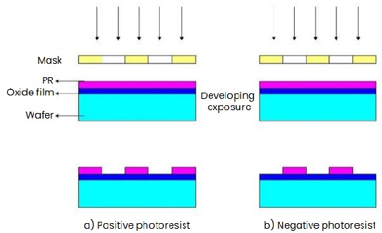
1) Any photoresist that is mainly cross-linked under the irradiation of energy beams (light, electron, ion, etc.) is called negative photoresist. It has strong adhesion, high sensitivity, and relaxed development conditions, and is suitable for the production of low-integration devices.
2) Same conditions as above, under the irradiation of energy beams (light, electron, ion, etc.) is called positive photoresist. It has the advantages of high resolution, high contrast, insensitivity to standing wave effects, large exposure tolerance, low pinhole density and non-toxicity, and is suitable for the production of highly integrated devices.
In addition, the supporting reagents refer to reagents used in conjunction with photoresist in process manufacturing, mainly including tackifiers, diluents, edge removers, developers and stripping fluids.
5. Polishing Materials
If the chip wants to have high stability, it needs high-quality surface polishing to achieve global uniform planarization of the entire wafer. While polishing pads and polishing fluid are key consumables in this process, which directly affect the basic effect of the CMP process.
Chemical mechanical polishing (CMP) technology is one of the important processes in wafer manufacturing and is crucial for high-precision and high-performance wafers. Different from traditional purely mechanical or chemical polishing methods, the CMP process uses a combination of surface chemistry and mechanical grinding technology to achieve the removal of different materials at the micron/nano level on the wafer surface, thereby reaching the height of the wafer surface (Nano level ) planarization effect, allowing the next step of photolithography process to proceed better. The equipment and consumables used in this process include: polishing machine, polishing fluid, polishing pad, post-CMP cleaning equipment, polishing endpoint detection and process control equipment, waste treatment and testing equipment, etc.
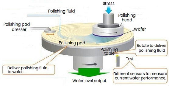
Figure 2: Chemical mechanical polishing (CMP) Technology
The main detection parameters of CMP equipment include:
1) Polishing rate: the total amount of wafer surface material polished per unit time.
2) Grinding uniformity: divided into intra-chip uniformity and inter-chip uniformity.
The former refers to the ratio of the standard deviation of a certain wafer's polishing rate to the polishing rate; while the latter is used to indicate the consistency of the polishing rate of the same wafer under the same conditions.
3) Amount of defects: for CMP, the main defects include surface particles, surface scratches, and abrasive residues, which will directly affect the product yield.
In order to achieve these performances, CMP equipment needs to apply a number of key advanced technologies such as nanoscale polishing, cleaning, online film thickness detection, and intelligent control.
Table 5: Application of CMP in the Semiconductor Industry
|
Applications
|
Productions
|
|
Medium
|
SiO2
BPSG
PSG
Polymer
Si3N4, SiOxNy
Aerosol
|
|
Metal
|
AI, AI alloy
Cu, Cu alloy
Ta
Ti
TiN, TiNxCy
W
Poly-Si
|
|
Substrate
|
Si
Sapphire
Compound semiconductor materials
|
|
Other
|
ITO
High K media
High Te superconductor
Optoelectronic materials
Plastic, ceramic
SOI
|
6. Sputtering Target Materials
It refers to a sputtering source that is deposited on a substrate to form various functional films through magnetron sputtering, multi-arc ion plating or other types of coating equipment under appropriate process conditions. That is, the material to be plated is called Sputtering target. Its manufacturing materials include metals, alloys, ceramic compounds, etc. Sputtering target is the main raw material for preparing electronic thin film materials by physical vapor deposition technology (PVD). It is mainly composed of target blank, backing plate and other parts.
(1) The target blank is the target material bombarded by high-speed particle beam and is the core part of the sputtering target. During the sputtering coating process, after the target is hit by ions, the atoms on its surface are sputtered out and deposited on the substrate to form an electronic film.
(2) The back plate mainly plays the role of fixing the sputtering target and involves the binding process. Due to the low strength of the target blank, the sputtering target material needs to be installed in a dedicated machine to complete the sputtering process. The inside of the machine is a high-voltage and high-vacuum environment. Therefore, the sputtering target blank needs to be bonded to the backing plate through different binding processes, while the backing plate needs to have good electrical and thermal conductivity.
There are many types of sputtering targets, which have different specifications even with same materials. According to different classification methods, sputtering targets can be divided into different categories. The main classifications are as follows:
Table 6: Sputtering Targets Types and Products for Semiconductors
|
Classification criteria
|
Product Category
|
|
Shape
|
Flat target, rotating target
|
|
Chemical Composition
|
Metal targets (pure metal aluminum, titanium, copper, tantalum), elemental non-metal targets (silicon, etc.), alloy targets (nickel-chromium alloy, nickel-cobalt alloy, etc.), ceramic compound targets (oxides, silicides, carbides, sulfides, etc.)
|
|
Application Fields
|
Semiconductor chip targets, flat panel display targets, solar cell targets, information storage targets, tool modified targets, electronic device targets, etc.
|
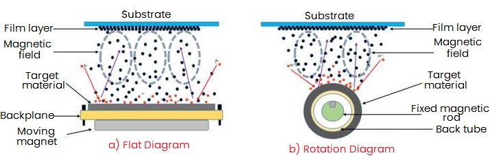
Figure 3: Schematic Diagram of Magnetron Sputtering
Sputtering targets are mainly used in the electronics and information industries, such as integrated circuits, information storage, liquid crystal displays, laser memories, electronic control devices, etc. Target materials commonly used in semiconductor chips include ultra-high purity aluminum targets, titanium targets, copper targets, tantalum targets, etc. They are mainly used to prepare key raw materials for ICs, with the highest technical requirements in terms of performance, ultra-high purity metals, size and high integration.
Packaging Materials
1. Die Attach Materials
Die attach materials play an important role in the chip manufacturing process. In chip packaging, they can do fixation, heat conduction, dust prevention and insulation to ensure the stable operation of the chip. They mainly have two categories: Organic and Inorganic
1) Organic materials have good plasticity and thermal conductivity, and are suitable for scenarios where packaging substrates are replaced multiple times, commonly used include epoxy resin, polyimide, etc.
Epoxy resin has excellent mechanical strength and electrical insulation properties and is widely used in the packaging of high-performance chips. While polyimide has a low dielectric constant and thermal expansion coefficient, making it suitable for chip packaging in high-frequency and high-temperature environments.
2) Inorganic materials mainly include:
Intermetallic compound materials such as silver paste and copper paste have excellent conductive properties and are widely used in the packaging of power chips.
Silicate materials have better high temperature resistance and packaging stability, and are suitable for chip packaging in high temperature environments.
2. Bonding Wire
Bonding wire is the core material for semiconductor packaging. It is a part that connects pins and silicon wafers and transmits electrical signals.
The wire bonding process is widely used to connect on-chip terminals to external leads of semiconductor devices. The connecting wires used in wire bonding are generally made of gold because of its anti-oxidation and high conductivity, and it can be easily bonded to designated locations through thermal compression and ultrasonic welding technology.
3. Ceramic Materials
Ceramics can provide higher resistance to heat, moisture, corrosion and electromagnetic interference, and can reduce electrical and thermal noise from electronic components inside the packages.
Current ceramic technology can already control the dimensional change of sintering within the range of 0.1%, and can be combined with thick film technology to create a multi-layer wiring conductive structure of 30-60 layers.
Advantages:
(1) In the packaging of various IC components, ceramic packaging can provide air-tight protection for the IC chips, making it have excellent reliability.
(2) Ceramics are extremely stable in terms of electrical, thermal, and mechanical properties, and their properties can be achieved by changing their chemical composition and process control and adjustment. They can not only be used as packaging capping material, but also an important carrier substrate for various microelectronic products.
Disadvantages:
(1) Compared with plastic packaging, its process temperature is higher, so the cost is higher.
(2) Process automation and thin packaging capabilities are inferior to plastic packaging.
(3) It has high brittleness and is prone to stress damage.
(4) In packaging that requires low dielectric constant and high wiring density, it must compete with thin film packaging technology.
4. Lead Frame
As the chip carrier of ICs, the lead frame is a key structural component that uses bonding materials (gold wire, aluminum wire, copper wire) to electrically connect the chip's internal circuit terminals and external leads to form an electrical circuit. When it comes to connecting to external wires, most semiconductor integrated blocks require the use of lead frames, which are important basic materials in the electronic information industry.
It is mainly produced by die stamping method and chemical etching method. The raw materials used in lead frames include: KFC, C194, C7025, FeNi42, TAMAC-15, PMC-90, etc.
5. Packaging substrates
The packaging substrate accounts for the largest cost of packaging materials and mainly plays the role of carrying and protecting the chip and connecting the upper chips and the lower circuit boards. It is used to assemble circuit components, resistors, capacitors, transistors, etc. together to protect and fix the components while providing electrical connections and signal transmission functions.
The packaging substrate subdivision process corresponds to different products and can be mainly divided into three levels:
1) Entry-level products include CSP, PBGA, used in chipsets, DRAM, and Flash products.
2) The general category includes FCCSP and FCBGA (non-CPU category), which can be used for communication chipsets and SiP packaging modules.
3) The high-end category includes complex FCBGA (CPU category) products, which can be used in CPU, GPU and other products.
6. Materials for Cutting
A wafer must go through three changes before it can become a real semiconductor chip: firstly, cut the block-shaped ingot into wafers; secondly, engrave the transistors after the previous process; and finally have packaging, a cutting process that turns the wafer into a complete semiconductor chip. In this process, the wafer will be cut into several hexahedral-shaped individual chips, called "Singulaton", and the process of sawing the wafer into independent rectangular parallelepipeds is called "Die Sawing".
The earliest wafer cutting method was physical cutting, using a dicing knife to divide the wafer into square chip dies. Nowadays, using diamond grinding wheel scribing knife is the mainstream method. And the new type of laser cutting is non-contact dicing, which does not produce mechanical stress on the wafer, causes less damage to the wafer, and can avoid problems such as chip breakage and damage.

 English










