Si & Ge Semiconductor
Silicon Semiconductors
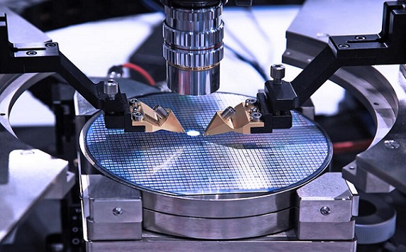
The first-generation semiconductor materials mainly include silicon (Si) and germanium (Ge), which are widely used in low-voltage, low-frequency, and low-power scenarios such as integrated circuits. However, it is difficult to meet the needs of high-power and high-frequency devices.
Semiconductor Si materials include silicon polycrystalline, silicon single crystal, silicon wafer, silicon epitaxial wafer, amorphous silicon thin film, etc., which can be used to prepare semiconductor devices. For the most semiconductor devices, the silicon material used is not silicon polycrystalline, but high-integrity silicon single crystal. It usually produced from silicon polycrystals by the Czochralski method or the zone melting method. After slicing, grounding or polishing (see semiconductor wafer processing), it is provided to device manufacturers for use.
Silicon has a gray metallic luster, is brittle, and has a hardness of 6.5Mohs, which is slightly lower than that of quartz. Its melting point is 1410°C, and the volume shrinkage rate is 9.5%. At room temperature, the surface of silicon is covered with a very thin oxide layer, which is chemically inactive. It reacts with oxygen at high temperature to form an amorphous silicon dioxide layer, which is often used as a masking layer and isolation layer in the devices.
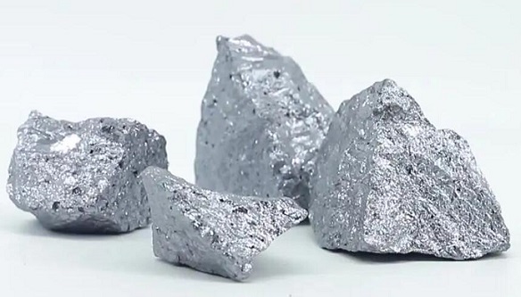
Silicon: As the most widely used semiconductor material, its advantages are as follows:
1) The silicon is rich in underground, so the cost of raw materials is low.
2) After decades of development, the purification process of Si has reached a very high level.
3) The interface of Si/SiO2 can be obtained by oxidation, which is very perfect. An extremely perfect interface can be obtained by post-annealing process.
4) The doping and diffusion process of Si has been studied extensively, and there is a lot of previous experience.
Disadvantages: On the one hand, the electron and hole migration speed of silicon is difficult to meet the needs of higher performance semiconductor devices in the future. Due to the low dielectric constant of silicon oxide, when the device is miniaturized, it will face the problem of dielectric material breakdown. Thus the replacement of dielectric materials is necessary. On the other hand, silicon is an indirect band gap semiconductor, and the light emission efficiency is not high.
Germanium Semiconductors
Germanium (Ge) is an important raw material for the semiconductor industry. Although Ge is a metal, it has many properties similar to non-metals, so it is called "semi-metal" in chemistry. In terms of its conductivity, it is superior to general non-metals and inferior to general metals, so it is also called a semiconductor in physics. Ge can be used in diodes, crystal triodes and compound transistors, photoelectric devices, Hall and piezoresistive sensors, radiation detectors, etc., and can also be used in color TVs, computers, telephones and high-frequency equipment. In addition, when the temperature changes, Ge's resistance also changes sensitively immediately, so it can be used to make thermistors. Now the Ge applications in semiconductor devices has been mostly replaced by Si, and only a certain amount is used in high-frequency and high-power devices, and the photoelectric avalanche diode is used in a large amount among them.
Germanium: As the earliest semiconductor material studied, the advantages of germanium are as follows:
1) The hole mobility is the largest, four times that of silicon; and the electron mobility is twice that of silicon.
2) The bandgap width is relatively small, which is conducive to the development of low-voltage devices.
3) The activation temperature is much lower than that of silicon, which is beneficial to save the thermal budget.
4) The small Bohr exciton radius helps to improve its field emission characteristics.
5) The small forbidden band width helps to combine dielectric materials and reduce leakage current.
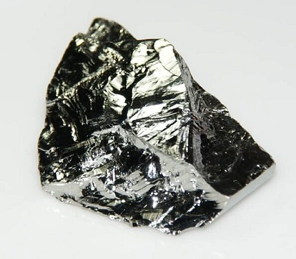
Disadvantages: Germanium is a relatively active material, and the interface between it and the dielectric material is prone to oxidation-reduction reactions, forming GeO, resulting in more defects, and then affecting the performance of the material. Due to the small reserves of Ge, it is not suitable to directly use it as the substrate. So semiconductor devices must be manufactured by GeOI (germanium on insulator) technology, but this has certain difficulties.
In the early 1950s, germanium was the most dominant semiconductor material, but since the early 1960s, silicon has replaced it as the main material for semiconductor manufacturing. The main reason why people use silicon today is because of the technique breakthrough in the silicon device process. In the silicon planar process, the use of SiO2 plays a decisive role in it. Economic considerations are also one of the reasons. It can be used to manufacture device-level silicon, which is far cheaper than other semiconductor materials. In addition, the content of silicon in silicon dioxide and silicate accounts for 25% of the earth, second only to oxygen. Silicon is arguably by far the most studied and most technologically mature semiconductor element on the periodic table.
Which is Better? Si vs Ge
1. At room temperature, silicon crystals have fewer free electrons than germanium crystals, which means that silicon has a much smaller collector cut-off current than germanium (the leakage current between the collector and emitter when the base is open, called through current).
2. Compared with Ge, Si collector cut-off current changes less with temperature.
3. The structure of Ge crystals is more easily damaged by high temperature, and silicon crystals are not easily damaged by overheating (the highest working junction temperature of Si is 150°C, while germanium is only about 60°C).
4. The peak reverse voltage rating (PIV) of silicon diodes is greater than that of Ge diodes.
5. The Si element is more abundant and the cost is lower.
6. A SiO2 layer is easily grown on the silicon surface and is technically easy to process, very useful for forming transistor gates (between the gate and the channel). Additionally, it acts as a masking layer, preventing dopant diffusion in the protected areas. In contrast, Ge does not form oxide layer easily on its surface.
7. The Si diode is larger than the Ge barrier (also called the potential barrier, which is formed by the diffusion of electrons and holes in the PN junction, and the potential difference on both sides). Looking at the structure of silicon, where electrons are tightly bound to atomic nuclei, it takes more energy to detach the electrons from the bonds to cross the barrier, and needs to apply more voltage to overcome the built-in voltage to start conduction.
As for development, the first transistors were made of germanium, but all things considered from above analysis, silicon was a better fit. However, germanium diodes have a turn-on voltage of 0.2V, which is more suitable for small signals.
GaAs Semiconductor
The second-generation semiconductor material is mainly gallium arsenide (GaAs), which is the compound material for making semiconductor light-emitting diodes (LEDs) and communication devices. However, GaAs materials have a small band gap, low breakdown electric field, but they are toxic, and can’t employed in high temperature, high-frequency and high-power devices.
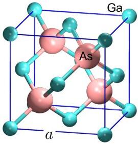
GaAs is an inorganic compound, and it is a dark gray solid, in addition, its melting point is 1238°C. It can exist stably in the air below 600°C and is not corroded by non-oxidizing acids. GaAs can be made into a semi-insulating high-resistance material whose resistivity is more than 3 orders of magnitude higher than that of Si and Ge, and is used to make integrated circuit substrates, infrared detectors, gamma photon detectors, etc. GaAs semiconductor devices have the advantages of good low-temperature performance, low noise, and strong radiation resistance. However, the magnification of the crystal triode made of it is small, the thermal conductivity is poor, and it is not suitable for making high-power devices. Compared with Si, GaAs is a material with a direct energy gap, so it can be used to emit light.
GaAs can process photoelectric data on one chip at the same time, so it is widely used in many optoelectronic fields such as remote control, mobile phone, DVD computer peripherals, lighting and so on. In addition, because its electron mobility is 6 times higher than that of silicon, gallium arsenide has become an important material for ultra-high-speed, ultra-high-frequency devices and integrated circuits.
SiC Semiconductor
A Short Brief
The third-generation semiconductor material is represented by silicon carbide (SiC). Compared with the previous two semiconductor materials, the biggest advantage of it is a wider band gap, which ensures that it can break down a higher electric field strength, so is suitable for the preparation of high-voltage, high frequency power devices. Devices made of SiC have the characteristics of high temperature resistance, high voltage resistance, high frequency, high power, energy saving, long life, and sound radiation resistance. They also have the advantages of fast switching speed and high efficiency, which can greatly reduce product power consumption, improve energy conversion efficiency and reduce the product size and have a wide range of downstream applications.
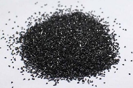
SiC is very hard, with a Mohs hardness of 9.5, second only to the hardest diamond in the world (grade 10). It has excellent thermal conductivity and can resist oxidation at high temperatures. Its advantages include stable chemical properties, high thermal conductivity, small thermal expansion coefficient, and strong wear resistance. Due to its high thermal conductivity, high breakdown electric field strength and high current density, many people try to use it to replace silicon in the application of high-power components.
SiC Advantages
1) High rated voltage: Whether it is a unipolar or bipolar device, the rated voltage of SiC devices is much higher than that of Si devices of the same type.
2) Low on-resistance: At 1kV voltage level, the on-resistance of SiC unipolar devices is 1/60 of that of Si devices.
3) High switching frequency: Set the maximum junction temperature at 175°C and voltage at 10kV, the SiC device can reach the maximum switching frequency of 33kHZ.
4) Low thermal resistance: The thermal conductivity of SiC devices is three times that of Si, and the internal heat is easier to dissipate, reducing the risk of device overtemperature failure and improving reliability.
5) Strong radiation resistance: Excessive radiation will not affect performance of SiC devices, so SiC is widely used in the aviation field.
Will the Future Be all Over for SiC and GaN?
Current fabrication technologies limit the cost-effectiveness of SiC and GaN compared to silicon, making both high-power materials expensive in the short term. However, both materials offer powerful advantages in specific semiconductor applications.
SiC may be a more marketable option in the short term because it is easier to manufacture larger, and uniform wafers than GaN. Over time, GaN will find its place in small high-frequency products due to its high electron mobility. Considering SiC's power capability and higher thermal conductivity, SiC will be more suitable for higher power products.
SiC power semiconductor devices include diodes and transistors, of which diodes mainly include junction barrier Schottky power diodes (JBS), PiN power diodes and mixed PiN Schottky diodes (MPS); while transistors mainly include metal oxide semiconductor field effect transistors (MOSFET), bipolar transistor (BJT), junction field effect transistor (JFET), insulated gate bipolar transistor (IGBT) and gate turn-off thyristor (GTO), etc.
SiC Applications
1) RF Devices
RF devices are components responsible for signal conversion in the field of wireless communication, such as power amplifiers, radio frequency switches, filters, low noise amplifiers, etc. GaN-on-SiC RF devices have the advantages of high thermal conductivity, high frequency, and high power. Compared with traditional silicon-based LDMOS devices, they can better adapt to low energy consumption, high efficiency requirements.
2) Power Devices
Also known as power electronic devices, they are mainly used in high-power electronic devices for power conversion and control circuits of power equipment, including diodes, transistors, thyristors, MOSFETs, IGBTs, etc. SiC devices have far-reaching influence in the medium and high voltage fields above 1000V. The main application fields are electric vehicles/charging piles, photovoltaic devices, rail transit, smart grid, etc.
3) New Energy Vehicles (NEV)
The components of the electric vehicle system involving the application of power semiconductors include motor drive systems, on-board chargers (OBC), on-board DC/DC and off-board charging piles. Among them, silicon carbide power devices are the most widely used in the market. The use of SiC modules makes the vehicle have lower energy consumption, smaller size, lighter weight, and longer mileage. In addition, the largest market share are vehicle inverters, almost 80%. In comparison, as for traditional IGBTs and inverters, the battery life of electric vehicles can only be increased by 5%, which is not obvious. However, if an 800V battery and a SiC inverter are used, the battery life will increase by 12%, whose improvement effect is relatively large.
4) Photovoltaic Power Generation
At present, leading photovoltaic inverter companies have replaced Si devices with SiC mosfet power devices. Based on the analysis data, the use of SiC power devices can increase the conversion efficiency to more than 99%, reduce energy loss by more than 50%, and increase the life cycle of equipment by 50 times, thus bringing the benefits of low cost and high efficiency.
5) Smart Grid
UHV power transmission projects have a major demand for SiC power devices. Its main application scenarios in the smart grid include: high-voltage DC transmission converter valves, flexible DC transmission converter valves, flexible AC transmission devices, high-voltage DC circuit breakers, power electronic transformers and other devices. Compared with general power electronic devices, power systems require higher voltage, greater power capacity and higher reliability. SiC devices break through the limitations of traditional power Si semiconductor devices in terms of high voltage, high power and high temperature. They have unique advantages such as high frequency, high reliability, high efficiency, and low loss, which promote the development of smart grids in applications such as solid-state transformers, flexible AC transmission, flexible DC transmission, high-voltage DC transmission, and power distribution systems.
6) Rail Transit
Here SiC used for traction converters, auxiliary converters, main and auxiliary integrated converters, power electronic transformers, power chargers and other devices.
7) Radio Frequency Communication
SiC and GaN radio frequency devices have both the high thermal conductivity and high-power radio frequency output compared to a single one. They can meet the requirements of 5G communication for high-frequency performance and high-power processing capability, and gradually become the mainstream technical route of 5G power amplifiers, especially macro base station power amplifiers.

 English