The 555 timer is an integrated circuit chip that is often used in timer circuits, pulse generators and oscillator circuits. It can be used as a delay device, trigger or oscillation element in the circuit.
555 Timer Basic
555 Timer Internal Block Diagram
The basic block diagram and pinout of the 555 timer is shown below. It is usually available in an 8-pin DIP package. While the basic 555 timer circuit consists of 2 comparators, voltage divider circuit, flip-flop, discharge transistor and output circuit.
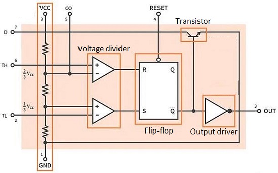
Figure 1: 555 Timer Internal Block Diagram
Part 1: Voltage Divider Circuit
The voltage divider for this circuit consists of 3 resistors of 5k. Since they have the same value, equal voltages are distributed between them, and the voltage across the resistors serves as the reference voltage for the comparator.
Part 2: Comparator
The comparator is a type of operational amplifier that mainly compares the voltage at the input terminal and outputs a high voltage or a low voltage according to the inverting input or non-inverting input.
* Circuit Analysis
1) The input of the up comparator (threshold) is the threshold pin connected to the non-inverting input (+) and the reference voltage of 2/3Ucc is connected to the inverting input (-) of the comparator. Another external pin "Control Voltage" is connected to the inverting input of this comparator so that the reference voltage of 2/3Ucc can be overridden and also the width of the output signal can be varied.
2) For the down comparator (trigger) 1/3 Ucc reference voltage is provided to the non-inverting input and the trigger pin is connected to the inverting input of the comparator.
The output of the comparator serves as the input to the flip-flop. While the SR flip-flop is a storage element that can store and output logic "0" or logic "1" according to two inputs SEF and RESET or S and R respectively. The output of the flip-flop is supplied to the output driver circuit to increase the current level and finally passed to the external output pin of the IC.
555 Timer Pins and Its Functions
|
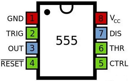 (source Wikipedia)
|
|
Pin
|
Name
|
Description
|
|
1
|
GND
|
Ground, connects the negative (0v) supply rail.
|
|
2
|
TRIG
|
Trigger, when the voltage of this pin drops to 1/3VCC (or the threshold voltage determined by the control terminal), the output terminal gives a high level.
|
|
3
|
OUT
|
Output, outputs high level (+VCC) or low level.
|
|
4
|
RESET
|
Reset, when this pin is connected to high level, the timer works. When this pin is connected to ground, the chip is reset and outputs low level.
|
|
5
|
CTRL
|
Control Voltage, controls the threshold voltage of the chip. (When this pin is left empty, the default two threshold voltages are 1/3VCC and 2/3VCC).
|
|
6
|
THR
|
Threshold, when the voltage of this pin rises to 2/3VCC (or the threshold voltage determined by the control terminal), the output terminal gives a low level.
|
|
7
|
DIS
|
Discharge, built-in OC gate is used to discharge the capacitor.
|
|
8
|
VCC
|
Supply +Vcc, provide high level and power the chip.
|
Functions
|
Input
|
Output
|
|
Threshold input (V11)
|
Trigger input (V12)
|
Reset RD
|
Output(Vo)
|
Discharge Tube TD
|
|
x
|
x
|
0
|
0
|
ON
|
|
< 2/3VCC
|
< 1/3VCC
|
1
|
1
|
OFF
|
|
> 2/3VCC
|
> 1/3VCC
|
1
|
0
|
ON
|
|
< 2/3VCC
|
> 1/3VCC
|
1
|
Unchanging
|
Unchanging
|
Working Principle
Part 1: Voltage Divider Circuit and Comparator Circuit
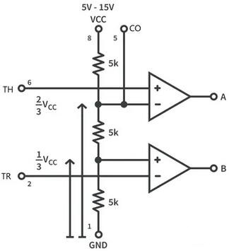
Figure 3: Voltage Divider Circuit and Comparator Circuit
The action of the 555 timer is controlled by 3 input pins: threshold, trigger and control voltage.
1) When the voltage on the Threshold pin increases above 2/3 Ucc reference voltage, you get a logic "1" at the output "A", otherwise, it is logic "0".
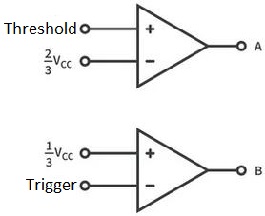
Figure 4: Threshold Comparator and Trigger Comparator
2) When the voltage on the trigger pin is less than 1/3Ucc reference voltage, you get logic "1" at the output "B", otherwise, it is logical "0".
Part 2: SR Flip-flop Circuit and Output Driver Circuit
The flip-flop has two inputs: the output of the threshold comparator labeled bit "A" is connected to R, and the output of the flip-flop labeled "B" is connected to S.
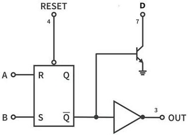
Figure 5: SR flip-flop and Output Driver Circuit
Below is the truth table for a basic SR flip-flop. When the SET or S input is logic "1", the set flip-flop outputs logic "1", and when the RESET pin is logic "1", the flip-flop outputs logic "1". When S and RESET are both logic "0", the flip-flop stores the previous value or acts as a storage element.; when both are logic "1", the flip-flop enters the invalid operation state.
|
S
|
R
|
Q
|
QBAR
|
|
0
|
0
|
Storage
|
Storage
|
|
1
|
0
|
1
|
0
|
|
0
|
1
|
0
|
1
|
|
1
|
1
|
Invalid
|
Invalid
|
The following is an analysis of the case where only one input is a logic "1" and the other is a logic "0". The figure below shows how the outputs of comparators A and B affect the output of the flip-flop. But there is a point to note here, get the output of the flip-flop from QBAR instead of Q.
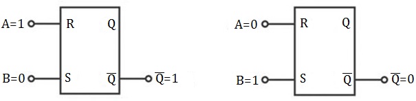
Figure 6: Flip flop
The flip-flop output depends on the input. It is passed to an output driver circuit, which increases the current level to drive loads up to 200mA, allowing the load to be connected directly to the IC's output. There is also a key point to note here. The output driver circuit is an inverting circuit, inverting the logic of QBAR. So in the end we get the same logic as the Q output of the flip-flop. And the flip-flop output is connected to the base of a discharge transistor, which is used to "discharge" any externally connected capacitance.
Operation Modes
The 555 timer has three working modes: monostable, bistable and astable. Various combinations of capacitors and resistors are connected to the input pins of the 555 timer so that it can be switched between the 3 modes. This way, if you create a different application using the 555 timer, you only need to rearrange the externally connected components.
1) Monostable Mode
Monostable is also known as "one-shot" mode. When triggered, it is timed to generate only one output pulse and return to a stable state. Uses include time delay generation, touch switches, pulse width modulation, etc.
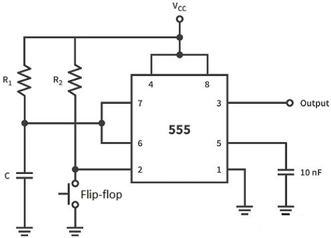
Figure 7: Monostable Mode
2)Bistable Mode
In this mode the timer acts as a flip-flop and since there are 2 stable modes it is possible to use the timer to store 1 bit of data, but this is not the preferred method of storing data.
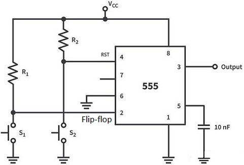
Figure 8: Bistable Mode
3)Astable Mode
In this mode, the 555 timer acts as an electronic oscillator. The output switches from a logic high connection to a logic low according to the configured period. Uses include pulse generation, logic clock generation, LEDs and flashes.
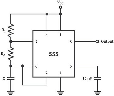
Figure 9: Astable Mode
555 Timer Application Example : LED Light
When we press the switch, the LED light will light up for a few seconds, and finally turn off automatically. How to use a 555 timer to make it?
The LED flicker made with 555 timer belongs to an astable mode. To make the LED lights turn off regularly, you must use its monostable mode. When it is working, it always outputs a low level, and when we press the switch, it outputs a high level for a period of time, and then automatically returns to a low level and maintains it.
The following is the circuit schematic diagram. When we power it up, its output is low level and the LED light is always off.
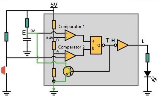
Figure 10: LED Light Circuit Schematic Diagram
Because this output buffer inverts the result, point T should be high level at this time; the transistor is turned on at this time, and the voltage at point E can be regarded as 0V. While the voltage at point B is 3.4V, for comparator 1, the reverse voltage is greater than the non-inverting voltage, so it outputs a low level. In the same way, comparator 2 also outputs low level. If both are low level, the flip-flop will remain in this state.
When we press the switch and loosen it immediately, the voltage at point F is 0V. For comparator 2, the non-inverting input terminal is greater than the inverting terminal at this time, so it outputs 1. For the flip-flop, S is 1 and R is 0, so it outputs high voltage; but this small circle will invert the result, so point T is low level; and it will be inverted again later, the final output is high level, and the LED light is on.
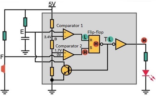
Figure 11: LED Light is ON
When the button is released, even if the voltage at point F changes to 5V, the output of the flip-flop is still high, because the inverting phase of comparator 2 is greater than the non-inverting phase, so its output is low level. Both are low levels for the flip-flop, so its state will not change.
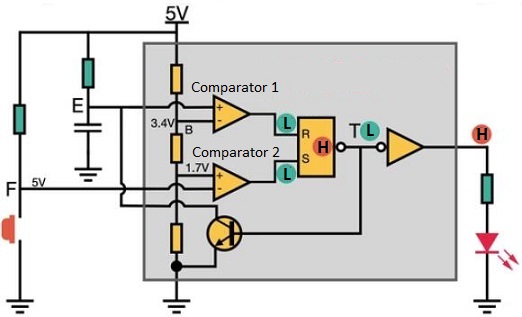
Figure 12: The LED Light Stays on After Releasing the Button.
Because the T point is low level, the transistor is cut off, which is equivalent to an open circuit. At this time, the power supply begins to charge the capacitor. When it is charged to 3.4V, the non-inverting phase of comparator 1 begins to be greater than the inverting phase, so its output is high level. For the flip-flop, R is 1 and S is 0 at this time, so it outputs a low level. After two inversions, its final output is also a low level, so the LED light turns off.
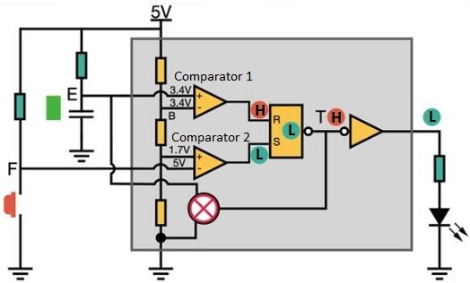
Figure 13: LED Light is OFF
At this time, point T is high level, so the transistor is turned on again, the capacitor begins to discharge through the transistor, and point E will be less than 3.4V, so comparator 1 begins to output low level again. Even if it outputs low level, the flip-flop has no effect, because its two inputs are both low level, and it will always maintain the previous state, that is low level. If we don't press the switch it will stay on.
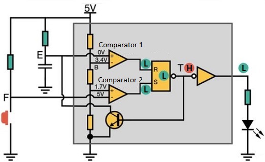
Figure 14: Output Low Level
Finally, let’s talk about how to calculate the delay time of LED lights. When we press the switch, the LED light is on, and when the capacitor is charged to 2/3 of the power supply voltage, the LED light is off. This is the calculation formula for the delay time t. If we want to delay for 3 seconds, we only need to choose a 10K resistor and a 273uf capacitor.
Alternative ICs
There are many alternative models of 555 timers produced by different companies, include different pin functions, and some use CMOS designs.
|
Manufacturer
|
Model
|
Remarks
|
|
Avago Technologies
|
Av-555M
|
*
|
|
Custom Silicon Solutions
|
CSS555/CSS555C
|
CMOS chip, minimum operating voltage 1.2V, IDD<5µA
|
|
CEMI
|
ULY7855
|
*
|
|
ECG Philips
|
ECG955M
|
*
|
|
Exar
|
XR-555
|
*
|
|
Fairchild Semiconductor
|
NE555/KA555
|
*
|
|
Harris
|
HA555
|
*
|
|
IK Semicon
|
ILC555
|
CMOS chip, minimum operating voltage 2.0V
|
|
Intersil
|
SE555/NE555
|
*
|
|
Intersil
|
ICM7555
|
CMOS
|
|
Lithic Systems
|
LC555
|
*
|
|
Motorola
|
MC1455/MC1555
|
*
|
|
National Semiconductor
|
LM1455/LM555/LM555C
|
*
|
|
National Semiconductor
|
LMC555
|
CMOS chip, minimum operating voltage 1.5V
|
|
NTE Sylvania
|
NTE955M
|
*
|
|
RCA
|
CA555/CA555C
|
*
|
|
STMicroelectronics
|
NE555N/ K3T647
|
*
|
|
TI
|
SN52555/SN72555
|
*
|
|
TI
|
TLC555
|
CMOS chip, minimum operating voltage 2.0V
|
|
Zetex
|
ZSCT1555
|
*
|
|
NXP
|
ICM7555
|
*
|
|
HFO / East Germany
|
B555
|
*
|
|
Hitachi
|
HA17555
|
CMOS
|
* 556 Dual Timer
The model that integrates two 555 timers in one chip is 556, and it includes 14 pins.
* 558 Quad Timer
The model that integrates four 555 timers in one chip is 558. And it includes 16 pins, of which four 555 timers share power, ground, and reset pins. The discharge pin and the threshold pin are combined into one pin and is called "timing". At the same time, the trigger pin is changed to falling edge trigger.

 English










