CMOS refers to a technology used to manufacture large-scale integrated circuit chips. It is a RAM chip on the computer motherboard. Because of the readable and writable feature, it is used to save the data after the BIOS has set the computer hardware parameters. The CMOS manufacturing is similar to the general computer chips, mainly using the two elements silicon and germanium. So what is the specific process like?
Complementary Metal-Oxide-Semiconductor (CMOS)
CMOS Process Technology
In 1963, Wanlass and Sah first proposed the concept of complementary logic. In 1966, RCA Corporation demonstrated the performance of CMOS for the first time. With the invention of the local oxidation process of silicon, the reduction of mobile ion charges, the introduction of ion implantation and the improvement of photolithography technology, CMOS technology has been widely used. The circuit diagram of the CMOS inverter shown in Figure 1, no matter the input is high or low, only one MOS tube is in the conduction state, and a certain power consumption is generated when the input level jumps, so the CMOS process technology becomes the mainstream semiconductor manufacturing process technology.
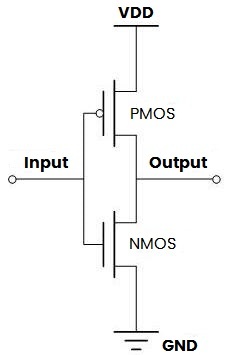
Figure 1: CMOS Inverter Circuit Diagram
The CMOS process has followed Moore's Law since its innovation, the size has been continuously reduced, and the integration level has been improved greatly. The changes in the CMOS feature size are shown in Figure 2.
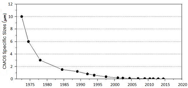
Figure 2: CMOS Specific Sizes
Basic CMOS Manufacturing Process
The 0.18μm process is a key node in the CMOS process. Above 0.18μm, CMOS is isolated by local oxidation of silicon (LOCOS) process and interconnected by metal aluminum (Al). 0.18μm uses shallow trench isolation (STI), and the retrograde well, also metal interconnection can be made of aluminum, but most of them use copper.
In semiconductor industry, the CMOS process is divided into front end and back end. The source and drain regions of the device are formed in the first stag, and the metal interconnection of the device is completed in the second stage. Here, taking the inverter as an example, first introduce the front-end process of the 0.18 μm CMOS process, and then introduce the back-end process of the metal Al interconnection.
The Front-end Process
1. Source Region
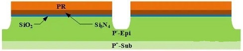
First, a layer of SiO2 is thermally oxidized and grown on the P-substrate/P-epitaxial layer, which is called the pad oxide. It used to relieve the stress between the subsequent growing Si3N4 and the silicon substrate. Because the lattice constants of Si3N4 and silicon do not match, there is a large stress between the two. If Si3N4 is in direct contact with silicon, it is easy to cause the silicon substrate to crack. Then deposit Si3N4, spin-coat photoresist (PR), and use mask photolithography to remove PR in the device isolation region, finally use acid etch to remove Si3N4, SiO2 and Si in turn to form a shallow groove of silicon, as shown in the Figure 3.
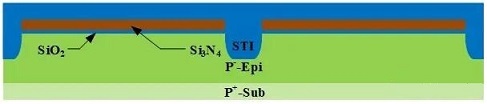
After that, thermally grow SiO2 (rounding oxide) at 1000°C. This step can make the sharp corners at the bottom of shallow trenches smooth, avoid breakdown voltage and reduce leakage current. Then SiO2 is deposited by low-pressure vapor phase, and the densification treatment is carried out at 950 °C under the atmosphere of O2 and N2, as shown in the Figure 4.
Use chemical mechanical planarization (CMP) to remove SiO2 on the surface until it reaches Si3N4, then use hot phosphoric acid (H3PO4) to etch away Si3N4, and finally remove SiO2 on the surface of the source region, as shown in the Figure 5.

2. N-well & P-well
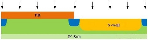
Next is ion implantation, as shown in Figure 6. Implant high-energy, high-dose (about 1013) impurity phosphorus (P) to form N-well, and implant low-energy (about 1012) arsenic (As) to prevent punch-through between PMOS source and drain punch through. Finally, low-energy As is injected into the order of 1011 to adjust the turn-on voltage of the PMOS.
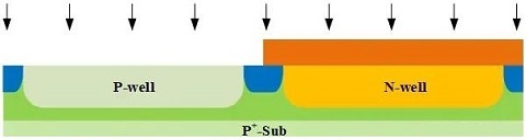
After that, high-energy, high-dose (about 1013) impurity boron (B) is implanted to form a P-well, and low-energy (about 1012) B is implanted to prevent NMOS source and drain punch through. Finally, the low-energy B is injected into the order of 1011 to adjust the turn-on voltage of the NMOS. The P and N wells are implanted three times, the energy and dose are from high to low, and the concentration distribution is from low to high from the surface of the silicon wafer. This kind of stuff is called a retrograde well, looking at Figure 7.
3. Grow and Remove Sacrificial Oxide
An sacrificial oxide layer of about 25nm is grown to capture defects on the silicon surface of the source region caused by ion implantation, as shown in the Figure 8.

Use HF solution to etch the sacrificial oxide layer, as shown in the Figure 9.

4. Formation of Oxide Layer and Gate
A 2-10nm gate oxide grow at 800°C, which is the most critical step in the process, and the thickness must be accurate to the order of Å, and then deposit polysilicon as the gate, as shown in the Figure 10.

After the polysilicon deposition is completed, gate photolithography is performed. With spin-coating PR and mask photolithography, and dry etching is used to form the gate and polysilicon interconnection of the device, as shown in the Figure 11.

Remove the PR and grow a thin oxide layer on the polysilicon surface to buffer and isolate the polysilicon and the formation of Si3N4, as shown in the Figure 12.

5. Lightly Doped Drain (LDD)
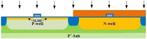
Mask performs photolithography treatment on LDD region of the NMOS source and drain, and then ion implants to form the NMOS lightly doped drain region (NLDD), as shown in Figure 13. The implanted element is As (about 1013), the injection energy is low, and the position is relatively shallow.
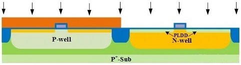
For PMOS lightly doped drain (PLDD) lithography and ion implantation, implant B element (about 1013), as shown in the Figure 14. Since the diffusion of B is faster than that of As, the implantation energy of PLDD is lower than that of NLDD.
6. Spacer
Deposit Si3N4 by CVD (chemical vapor deposition) method with a thickness of 120~180nm, as shown in the Figure 15.
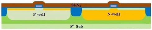
Etch the thin layer of Si3N4 on the horizontal surface by reactive ion etching (RIE), leaving the isolation spacer, as shown in Figure 16. Then take rapid thermal annealing (RTA) on the implanted LDD. While spacer is used as a barrier layer for subsequent implantation of S and D regions, which called a self-alignment process.

7. CMOS Source and Drain Production
Make NMOS area by spin-coat PR and mask photolithography, as shown in Figure 17. As elements are implanted with a dosage of about 1015 and an implantation energy of about 60KeV to form the source (S) and drain (D) regions of the NOMS.
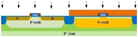
Make PMOS area by spin-coat PR and mask photolithography, as shown in Figure 18. Inject BF2+ ( about 1015), and the energy is lower than that of NMOS, forming S and D of PMOS.
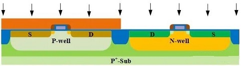
After the S and D of NMOS and PMOS are made, perform RTA to activate the implanted elements and eliminate the related damage, as shown in the Figure 19.

Remove the surface oxide, and flood the part in the hydrofluoric acid solution quickly to expose the silicon in the gate, source, and drain regions, as shown in the Figure 20.

8. Formation of Metal Silicides
In order to reduce the resistance of polysilicon, and the metal and polysilicon, metal salicide is generally used in the CMOS process. Titanium (Ti) or (Co) is mostly used. For example, a layer of Ti with a thickness of 20-40 nm is deposited on the silicon wafer by sputtering, as shown in the Figure 21.

Then RTA is carried out, and the metal and silicon react at high temperature to form a metal silicide, as shown in the Figure 22. For example, the area where Si and Ti are combined forms a metal silicide, and the Ti in other areas does not change, which is called a self-aligned metal silicide process.

Ammonium hydroxide + hydrogen peroxide wet etching is used to remove unreacted Ti, and the silicon-titanium alloy is retained, as shown in the Figure 23. Perform RTA again to reduce the resistance of the metal silicide.

Aluminum Interconnection
The back-end is mainly metal interconnection, where aluminum is introduced blew.
1. Contact
The preparation of CMOS devices is completed in the front-end process, and the interconnection between devices is carried out in the back-end. The 0.18μm CMOS dielectric is planarized by the CMP process, the metal tungsten (W) fills the holes, and the metal aluminum is used for interconnection.
The CVD method is used to deposit borophosphosilicate glass (BPSG) of about 1μm, silicon dioxide doped with a small amount of boron and phosphorus, which can improve the fluidity of the film and confine pollutants, insulating the device and the first layer of metal, as shown in the Figure 24.

After polishing by CMP process, a smooth BPSG surface is obtained, as shown in the Figure 25.

Through Spin-coat PR and mask photolithography, then define contacts, as shown in the Figure 26.
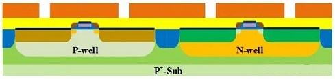
Use RIE (fluorine) dry etching to obtain spacer, provide link channels for metal and underlying devices, and remove PR, as shown in the Figure 27.

Deposit TiN with a thickness of about 20 nm, which helps the subsequent tungsten metal to adhere to the oxide layer, as shown in the Figure 28.
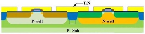
Metal tungsten is deposited by CVD method, and the contacts are filled with a thickness not less than half of the diameter of it, as shown in the Figure 29.

Use CMP to polish the surface metal tungsten and titanium nitride, leaving W to fill contacts, as shown in the Figure 30.

2. Metal1
It is deposited by a sputtering process, which consists of several different layers of metal, as shown in the Figure 31.
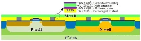
By Spin-coat PR and mask photolithography, define the Metal1 interconnection. Metal is etched by RIE. Since Metal1 is composed of multiple layers of metal, multi-step etching is required, and then PR is removed, as shown in the Figure 32.
3. Via Holes and Second Metal2
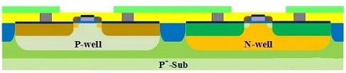
Use CVD to deposit undoped SiO2 metal insulator (IMD) material, fill between the metal lines, and provide insulation between the metal layers, as shown in the Figure 33.

Polish IMD by CMP, take spin-coats PR and mask lithography, and defines vias, as shown in the Figure 34.
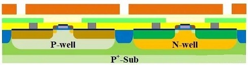
Use RIE (fluorine) to obtain spacer, get connection channels between metal layers, and remove PR, as shown in the Figure 35.
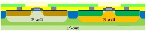
Now deposit a layer of TiN on the surface of Vias, and then deposit metal W to form a connection with Metal1.
Metal W and TiN CMP polishing treatment, as shown in the Figure 36.
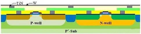
Like Metal1, Metal2 deposition increases in thickness and width, connects longer distances, and carries greater current, as shown in the Figure 37.
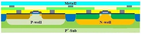
Etch Metal2, and remove PR, as shown in the Figure 38.

As for passivation layer deposition, there are a variety of it to choose from, such as SiO2, Si3N4 and polyimide, etc., as shown in the Figure 39. It protects the circuit from scratches, contamination, moisture, etc.
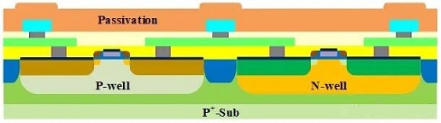
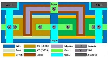
The passivation layer is etched to expose the pad window, which provides a point contact window for external power supply to the chip. The top view is shown in the Figure 40.

 English










