In semiconductor device fabrication, the IC patterning process includes Exposure, Develop, Etching and ion implantation and others. Among them, the etching process is the next step of the photo process, which is used to remove the bottom area not covered by the photoresist (PR). This process is designed to fix the mask pattern to the photoresist-coated wafer (exposure → development) and then transfer it back to the film layer under the PR. With the miniaturization of the critical dimension (CD) of the circuit (2D perspective), the etching process changes from wet etching to dry etching, so the required equipment and processes are more complicated. Due to the active use of 3D stacking methods, the core performance index of the etching process fluctuates, so the etching has become one of the important process flows in semiconductor manufacturing.
The photo process forms a pattern on the object to be etched. At this time, the photoresist is used as a masking layer for etching, or called masking film. In some cases, a hard mask is also used for etching. Next, put it into dry etching equipment. Here parameters that need to be adjusted include gas and its composition ratio, etching pressure, stage temperature, etc. During process, the resist will also be etched partly, and the ratio of the PR etching rate to the rate of the object to be etched is called etch selectivity.
In addition, the uniformity of the etching rate is also considered in the wafer, even the substrate can be seen, the process must continue, which is the so-called over etching. At this time, the substrate will also be partially etched.
Etching in Semiconductor Manufacturing
Development Trends of Deposition and Etching
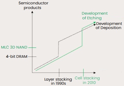
Figure 1: The Development Trends of Etching and Deposition Technology
The process of forming a "layer" on a wafer is called deposition (chemical vapor deposition (CVD), atomic layer deposition (ALD) and physical vapor deposition (PVD)), and then the circuit pattern is drawn on the "layer" is called exposure. And etching is the process of patterning the wafer following the deposition and exposure processes. The role of the photo process is similar to drawing a sketch, and it is the deposition and etching processes that really change the wafer significantly.
Both etching and deposition techniques have evolved significantly since the advent of semiconductors. The most striking innovation in deposition is the shift from Trench to Stack, which is similar to the development of device capacity from 1 megabit (Mb) DRAM to 4 megabit (Mb) DRAM in the early 1990s. Where a key node in etching was in the early 2010s, when the number of stacked layers of 3D NAND flash memory exceeded 24. As the number of stacked layers increases to 128, 256 and 512 layers, the etching has become one of the most technically difficult processes.
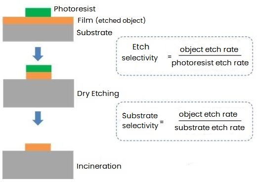
Figure 2: Dry Etching Technology Process
The Development of Etching Ways
Terminology
The same etching process corresponds to a variety of materials and graphics, and the requirements are different, so the etching processes are also different.
Materials: semiconductors, films (insulating films, metal films, etc.)
Gas: SF6, CHF3, CF4, C4F8, Cl2, BCl3, HBr, NF3, SiCl4, etc.; Ar, O2, He (auxiliary gas)
Simply put, the gas used in the etching can react with the object to be etched and generate volatile substances, but not any gas can be used. In addition, a gas should in a steady state. When using liquefied gas, it is necessary to set the configuration of the gasification and the appropriate temperature. Here we need to mention a point, etching deviation. The most advanced lithography equipment is very expensive. In order to give full play to its performance, it is very important to etch according to the size of the PR pattern, which is called anisotropic etching. This dimensional change before and after etching is called etching deviation. For wet etching using chemical reagents, the etching will be relatively large, which is called lateral etching.
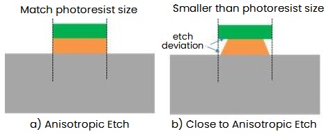
Figure 3: Dimensional Deviation in Etching
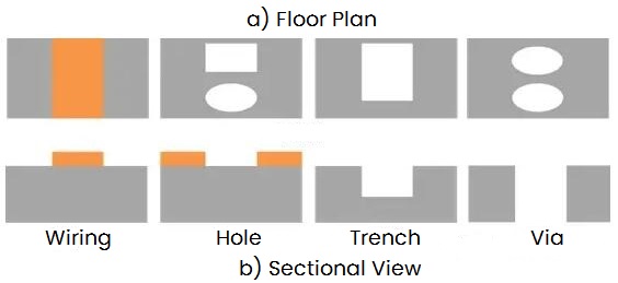
Figure 4: Etched Patterns
Semiconductor devices need to be etched into various shapes. Among them, there are wiring patterns, through holes for interconnection between lines, and trenches for separating components, etc.
Plasma
Plasma etching is inseparable from the generation of plasma, which is the fourth state of matter besides gas, liquid, and solid. Roughly speaking, it is an ionized gas whose overall charge can be considered neutral. Generally, the plasma used in semiconductor processes is low-temperature, which is different from the high-temperature one used in nuclear fusion.
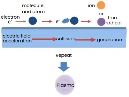
Figure 5: Plasma Generation
After forming a vacuum, introduce the desired gas, set the gas pressure required to generate the discharge, apply radio frequency to the electrode to discharge, and the generated electrons collide with the gas molecules, thereby generate ions and neutral active free radicals. Repeating them continuously will generate plasma, so it can be seen that etching is a vacuum process.
Typically, two parallel plate electrodes generate a plasma, where the difference in electrical potential is created by the difference in the mobility of electrons and ions in the plasma itself (sometimes called bulk plasma) and one near the electrodes. This is known as the plasma potential. The part where the potential change occurs between the bulk plasma (main plasma) and the substrate is called the sheath, which plays an important role in film formation and etching.
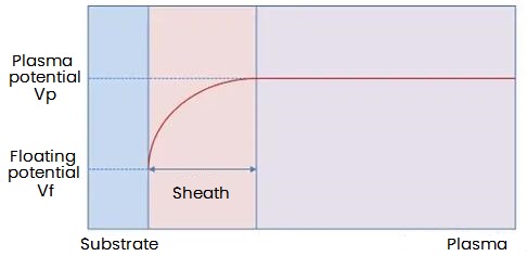
Figure 6: Plasma Potential
Also, one of the parameters representing the motion of particles in a gas is the mean free path. This is how far a particle travels after hitting another particle before hitting the next one, and is inversely proportional to the gas pressure. In other words, it represents the distance that particles in the gas can move, which is often seen in vacuum part.
Technological Evolution
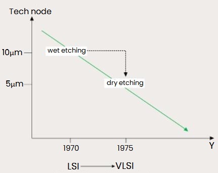
Figure 7: The Development of Etch Ways (2D)
During the development of 2D miniaturization and 3D stacking technology, the etching process is also following. In the 1970s, 2D semiconductors became the mainstream, and the critical dimension (CD) of circuits dropped rapidly from 100 microns (μm) to 10 microns (μm), or even lower. During this period, most of the key techniques in the semiconductor manufacturing have matured, and the etching has transitioned from wet etching to plasma etching. In the pass, for the ply cutting technique, the chemical wet method was first used, which is a relatively simple. Since it was difficult to meet the critical dimension requirement of 5 microns (μm) from the early 1970s, the plasma way was developed. Today, the etching process mostly adopts it, and the wet etching technology is later developed and applied to the cleaning process.
Advantages and Disadvantages
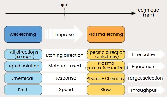
Figure 8: Wet Etching and Plasma Etching
Wet etching is faster because of the use of liquid, and the depth of removal per minute is greater, but it will not form a structure similar to a rectangle. And it etches all directions uniformly, resulting in loss in the lateral direction, which should be avoided for CD miniaturization. In contrast, plasma etching can cut in a specific direction, making it possible to achieve an ideal ultra-fine pattern profile at the nanometer (nm) level.
In addition, wet etching will cause environmental pollution, because the used liquid solution needs to be discarded after the process is completed. In contrast, with plasma etching, a scrubber is placed in the discharge line, which reduces the environmental impact by allowing the exhaust to go through a neutralization process before being released into the atmosphere.
However, due to the intricate intertwining of several layers above the wafer, it is difficult to target a specific layer (film) with this way. While having a specific layer, it is easier to use wet etching because it uses a chemical reaction to etch. By contrast, it is not easy to use the plasma method when performing selective etching, because a combination of physical and chemical techniques is required.
Etching Processes
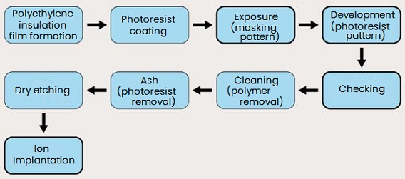
Figure 9: Etching Related Process
Let's sort it out, the etching process begins with forming a thin film, applying PR on it, and performing steps such as exposure, development, etching, ashing, cleaning, inspection, and ion implantation, etc. which are semiconductor manufacturing cores. If the PR cannot be cut smoothly during the developing process, the remaining will hinder the etching. If the target layer is not sufficiently etched, ions cannot be implanted as planned because of impurities. The same effect can occur if residual polymer is not completely removed after plasma etching. If the time control fails, the amount of ion gas in the plasma is too large or the film is over-etched, it will cause physical damage to the underlying film.
Therefore, it is very important to precisely control the end of point (EOP) during process. It is also very important to thoroughly check the etch conditions as well as the ashing and cleaning process. Wafers can be rejected if they are not etched uniformly, and under-etching is more bad than over-etching.
The Rise of Plasma Etching
Due to the complexity of the steps involved in the etch process, this article will give two parts. In this section, it describes the history and direction of etch technology. In the next section, you will get the relationship between plasma and etch, RIE, etch method, aspect ratio, and etch speed.
Early wet etching promoted the development of Cleansing or Ashing process. Today, the plasma etching (dry etching) has become the mainstream. Plasma consists of electrons, cations and radicals. The energy applied to the plasma strips the outermost electrons of the source gas in a neutral state, converting these electrons to cations. In addition, imperfect atoms in molecules can be stripped by applying energy to form electrically neutral free radicals. Dry etching utilizes cations and free radicals that make up the plasma, where cations are anisotropic (suitable for etching in a certain direction), and free radicals are isotropic (suitable for etching in all directions). The number of free radicals far exceeds the number of cations. In this case, the dry etch should have been isotropic like the wet etch. However, it is the anisotropic etching of dry etching that makes ultra-miniature circuits possible. In addition, the etching speed of cations and radicals is very slow, so how can we apply the dry etching to mass production in the face of this shortcoming?
(A/R) Aspect Ratio
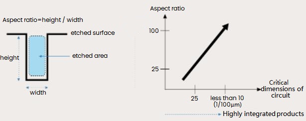
Figure 10: Aspect Ratio
Aspect ratio is the ratio of horizontal width to vertical height. The smaller the critical dimension (CD) of the circuit, the larger the aspect ratio value. That is, assuming an A/R of 10 and a width of 10nm, the height of the holes drilled during etching should be 100nm. Therefore, for next-generation products requiring ultra-miniaturization (2D) or high density (3D), extremely high A/R values are required to ensure that cations can penetrate the bottom film.
To achieve ultra-miniaturized technology with a critical dimension of less than 10nm in 2D products, the capacitive A/R value of DRAM should be kept above 100. Similarly, 3D NAND flash also requires higher values to stack 256 or more stacking layers. Even if the conditions required by other processes are met, the desired product cannot be produced if the etching process is not up to standard. This is why it is becoming more and more important in IC manufacturing.
Plasma Etching Brief
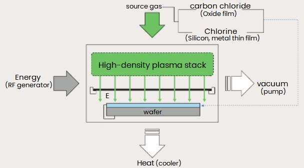
Figure 11: Plasma Source Gas Based on Films
When a hollow pipe is used, the narrower the diameter of the pipe, the easier it is for the liquid to enter, which is the so-called capillary phenomenon. However, if a hole is to be drilled in the exposed area (closed end), the entry of liquid becomes quite difficult. Therefore, dry etching has gradually replaced wet etching to have the circuit was 3 to 5μm in the mid-1970s. That is, although ionized, individual molecules penetrate deep pores more easily because their volume is smaller than that of organic polymeric solution.
During the plasma etching, before injecting the plasma source gas suitable for the relevant layers, the inside of the processing chamber for etching should be adjusted to a vacuum state. When etching solid oxide films, stronger fluorocarbon-based source gases should be used. For relatively weak silicon or metal films, a chlorine-based plasma source gas should be used.
So, how should the gate layer and the underlying SiO2 insulating layer be etched? First, for the gate layer, silicon should be removed using a chlorine-based plasma (silicon + chlorine) with polysilicon etch selectivity. For the bottom insulating layer, the silicon dioxide film should be etched in two steps by using a fluorine-based plasma source gas (silicon dioxide + carbon tetrafluoride) with a stronger etching selectivity and efficiency.
RIE (Reactive-ion Etching) Brief
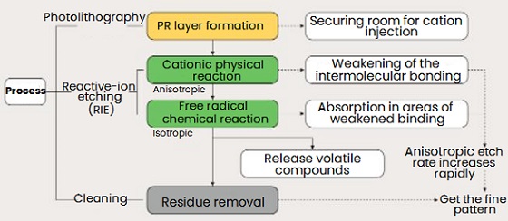
Figure 12: Advantages of RIE Method
Plasma contains both isotropic radicals and anisotropic cations, so how does it perform anisotropic etching? Plasma etching is mainly performed by reactive ions (RIE). The core of the RIE method is to weaken the binding force between target molecules in the film to attack the etched area. The weakened area is absorbed by free radicals, combines with the particles that make up the layer, and finally converts to a gas (a volatile compound).
Although free radicals are isotropic in character, the molecules that make up the underlying surface, whose binding force is weakened by the attack of cations, are more easily captured by free radicals and transformed into new compounds than the side walls with strong binding forces. Therefore, etch down becomes the mainstream. The trapped particles become a gas with free radicals, which are desorbed and released from the surface under the action of a vacuum.
At this time, the combination of cations obtained by physical action and free radicals obtained by chemical action is used for physical and chemical etching. Compared with the case of cation etching or free radical etching alone, the etching rate (within a certain period of time) degree of etching) increased by a factor of 10. This method can not only increase the etching rate of anisotropic down etching, but also solve the problem of polymer residue after etching.
Etch Rate and Related Index
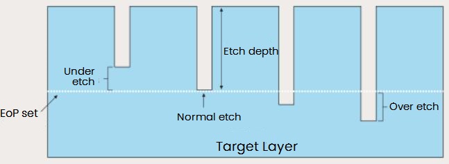
Figure 13: Main Etch Performance Index
The etching rate refers to the depth expected to be achieved by etching the film for one minute. So what does it mean that parts of a single wafer have different etch rates?
This means that various parts of the wafer are etched to different depths. For this reason, it is important to set EOP at which etching should stop by considering the average etch rate and etch depth. Even with that, there are still areas that are overetched or underetched than originally planned. However, during etching, under-etching is more damaging than over-etching. Because in the case of insufficient etching, the insufficiently etched part will hinder subsequent processes, such as ion implantation.
At the same time, selectivity is a key indicator of the etching. Its measurement standard is formulated according to the etching rate comparison between the mask layer (PR film, oxide film, silicon nitride film, etc.) and the target layer. And the higher the selectivity, the faster the target layer will be etched. The higher the level of miniaturization, the higher the requirements for selectivity to ensure that fine patterns can be perfectly rendered. Since the etching direction is straight, the selectivity of cationic etching is low, while the selectivity of radical etching is high, which improves the RIE.
Etch Details
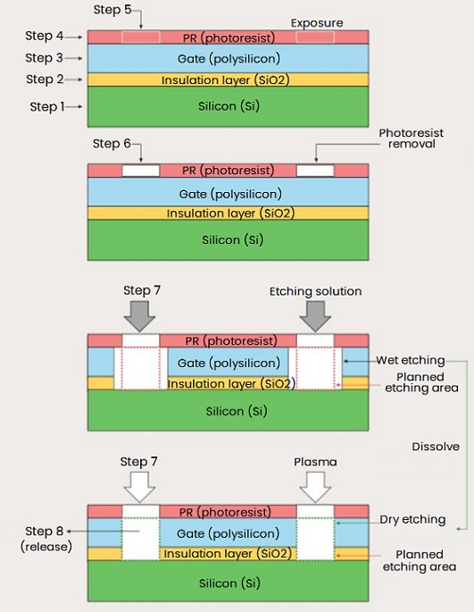
Figure 14: Etching Process Details
First, the wafer is placed in an oxidation furnace at a temperature between 800 and 1000°C, and then a SiO2 film with high insulating properties is formed on the surface of the wafer by a dry method. Next, it enters the deposition process to form a silicon layer or a conductive layer on the oxide film by chemical vapor deposition (CVD)/physical vapor deposition (PVD). If a silicon layer is formed, impurity diffusion may be performed to increase conductivity if necessary. During this process, multiple impurities are often repeatedly added.
At this time, the insulating layer and the polysilicon layer should be combined for etching. First, use photoresist, then a mask is placed on the photoresist film and subjected to wet exposure by immersion method, thereby imprinting the desired pattern on the film. When the pattern outline is rendered by development, the PR is removed from the photosensitive area. Then, the wafer processed by the photo process is transferred to the dry etching.
Both dry etching and wet etching are aimed at increasing the A/R value of the etching. In addition, regular cleaning is necessary to remove the polymer accumulated at the bottom of the hole. It is important that all variables such as material, source gas, timing, form and sequence should be organically adjusted to ensure that the cleaning solution or plasma source gas flows down to the bottom of the trench. So a small change in a variable requires recalculation of other variables, and this recalculation process will be repeated until it meets the requirements.
In addition, single-atom layers such as atomic layer deposition (ALD) layers are getting thinner and harder. Therefore, etching technology is developing towards the use of low temperature and low pressure. The etch process is designed to control the critical dimension to create fine patterns and ensure that problems caused by the etch process are avoided, especially under-etch and problems related to residue removal. The above content on etching are intended to give readers an understanding of the purpose of the etching, the obstacles to achieving the above goals, and the points used to overcome them.

 English










