Common-mode signals and rejection are very important for analog circuits and analog ICs. A common-mode signal is a signal acting on the non-inverting and inverting inputs of a differential amplifier or instrumentation amplifier. Referenced to the local common or ground, the common-mode signal appears on both wires of the two-wire cable with the same amplitude and phase. In electronic systems and communications, common-mode signals are a common source of interference.
Common-mode Rejection Analysis
1. Common-mode Signal
A common mode signal is a type of electrical signal that is present in both inputs of a differential amplifier at the same time and in the same phase. This means that the signal is the same voltage level on both inputs, and the point is, it is not the voltage difference between the two inputs that the differential amplifier is designed to amplify. So the common mode here refers to signals or noise that flow in the same direction in a pair of lines.
A differential amp has 2 inputs, with two copies of the same signal, opposite in phase is sent from the transducer to the 2 inputs of diff amp via 2 different wires. Any noise induced in the 2 wires due to the ambient electrical equipment etc are equal in amplitude and shape, so get subtracted wheres as the 2 copies of the required signals since opposite in phase. This is a clever way to outwit the effect of noise.
Case 1
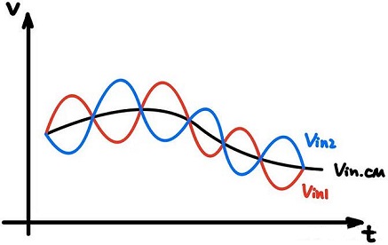
Figure 1: Vin
The bias voltages of the two input tubes are different and have their own operating points.
Case 2
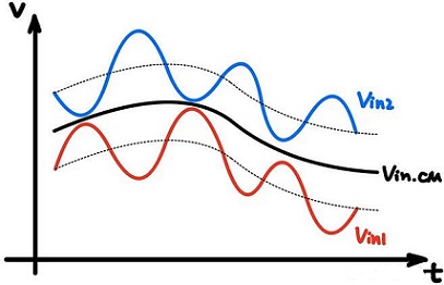
Figure 2: Vin
This situation is more complicated because the biases corresponding to the two input tubes are different.
2. Impact On Output
If the common-mode signal is regarded as a relatively slowly changing bias voltage, then the output common-mode voltage can be discussed using the method of large signal analysis. For example, let’s briefly analyze the large signal response of the CS-level amplifier circuit.
2.1 Low-frequency Response of CS-level Amplifier Circuit
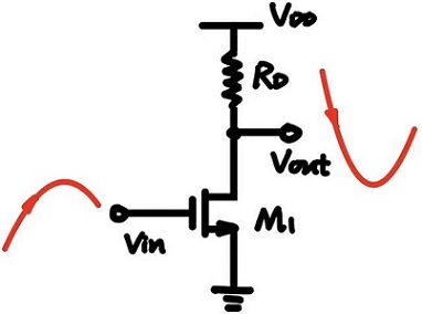
Figure 3: Input and Output (with amplification and inversion)
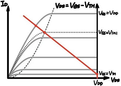
Figure 4: Three Important Nodes (as the bias voltage changes).
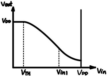
Figure 5: Low-frequency Relationship between Input and Output
If the input voltage here is regarded as a change in the bias voltage, then it is obvious that the output voltage will have a corresponding, slow, and inverse change. So when the common mode level (bias voltage of the input) changes, the level of the output point will also change. So how does common-mode rejection work, if not by preventing the common mode level from causing changes in the output? At this time, we will talk about the role of the differential amplifier.
2.2 Common-mode Rejection of Differential Pairs
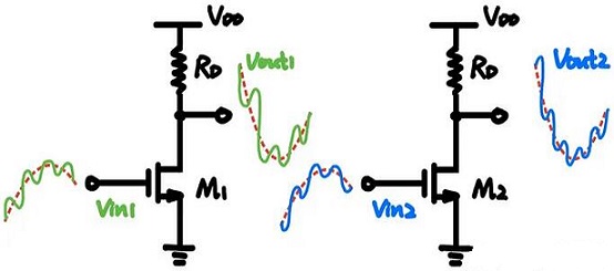
Figure 6: Common-mode Rejection of Differential Pairs
In Figure 6, although the input and output small signals fluctuate around a drastically changing operating point, as long as the green output and the blue output are subtracted, the changing red dotted line will be erased, and the opposite phase small fluctuations are preserved. It should be noted here that the differential input single-ended output (passive load differential pair) of a fully differential circuit not only loses gain, but also loses the function of eliminating common mode changes because there is no such subtraction process.
3. Add Tail Current Source
3.1 Ideal Current Source
As a small DC resistor and a large AC resistor, the most direct effect of the current source is to change half of the circuit from an ordinary CS stage to an active stage with negative feedback. Because we are discussing common-mode signals, and assuming that the circuit is completely symmetrical, we can think that each half of the circuit has one-half of the tail current flowing through it.
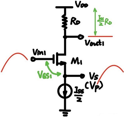
Figure 7: Voltage Change at Different Points
Note that there are commonly used formulas:

As long as the tail current does not change, Vgs does not change. This is a source follower. So how does its drain voltage change? Let's look at KCL for this circuit, where does the tail current come from? It can only come from the power supply. How many branches are there from the power supply to the tail current? There is only an overload resistor, so the voltage drop across the load resistor is fixed, then the output level is fixed. In this way, even if the input bias voltage changes greatly, the output voltage remains unchanged. In other words, the circuits on both sides are indeed dividing the tail current equally. As long as Iss/2 remains unchanged, the voltage drop of the drain resistor will remain unchanged, so does the output level. Looking back at the fully differential case, the voltage changes on both sides need to be taken into account.
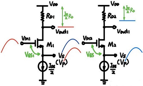
Figure 8: Ideal Tail Current Source
Note that at this time, the two output levels are different because the two load resistors are different. This is a small problem, because this fixed level does not provide information about the input changing common mode level, we can also think that the common mode signal is not passed to the output port. However, when this circuit processes differential signals, the gains of the circuits on both sides will be different. In short, an ideal tail current source can greatly suppress input common mode fluctuations.
3.2 Non-ideal Current Source
Use a biased MOS in the saturation region as a tail current source, and similarly consider half of the circuit.
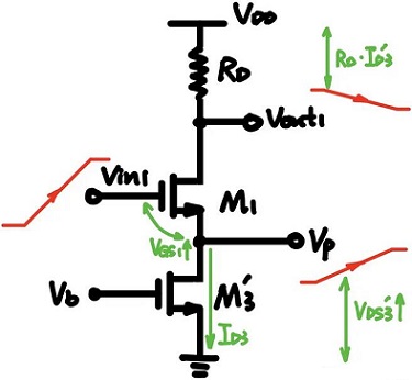
Figure 9: Voltage Changes at Each Point When the Tail Current Tube Has Channel Modulation
Note that the M3' tube is a virtual MOS used to generate half of the tail current, and the tube used to generate the full tail current is named M3. When M1 is understood as a source follower, Vp increases with Vin, Vgs remains unchanged and the absolute value is related to Ids. But now due to the modulation of the channel length of the tail tube, an increase in Vp is equivalent to an increase in the drain-source voltage, so the drain-source current Id3 of M3’ will increase. Let’s look back at Vgs1in the formula:

Where Vgs1 will increase, and Vp cannot keep up with the changes in Vin. But these changes have nothing to do with output, because as long as Vp changes, Id3 will change, then the current flowing through the drain resistor will change, and finally the output voltage will change. In Figure 9, Vp increases with Vin with a coefficient less than 1, so Id increases, causing the voltage drop on the resistor to increase and the output voltage to decrease. Therefore, changes in the input signal are reflected on the output port, and the common mode has an impact.
It is mentioned above that even if there is no tail current source to assist the output common mode, the violent fluctuations can be eliminated through the subtraction of the symmetrical circuit. What problems will there be at this time?
Let’s go back and look at the complete differential circuit:
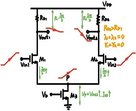
Figure 10: Common-mode Voltage
It can be found that different load resistors cause different changes in the voltage at the output point, then the difference between the voltages at the two points will no longer be zero, that is, the change in the common mode voltage at the input point is not only reflected in the common-mode voltage, and due to the asymmetry of the circuit, it is also reflected in the differential signal.
4. Rejection Reasons
1) Interference Suppression
Common-mode signals will be generated by environmental noise, power supply spurs, and grounding issues. If not suppressed, they can prevent correct recovery of differential signals, causing data errors or distortion.
2) Signal Integrity
The presence of common-mode signals may destroy signal integrity, such as causing clock jitter and reducing signal rise/fall times. By suppressing them, we can improve signal stability and integrity.
3) System Performance
Common-mode signals affects system performance and noise margin. By suppressing them, we can improve the system's dynamic range, signal-to-noise ratio, and sensitivity.
Common-mode Interference
Common-mode Interference refers to the interference signal between two signal lines and ground. Under normal circumstances, it has large amplitude and high frequency, and can also produce radiation through wires, causing a greater impact. As shown in Figure 11, when L and N produce lines with the same direction and different sizes relative to the earth, common-mode interference will occur.
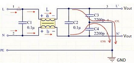
Figure 11: Common-mode Interference
By suppressing common-mode interference, on the one hand, prevent the impact of external signals on the circuit itself, and on the other hand, prevent the circuit itself from impacting external lines.
1) Common-mode Inductor
It is also called filter inductor, or common mode choke, which is used to suppresses common mode interference. For example, it is often used in computer switching power supplies to filter common mode electromagnetic interference signals. In PCB design, it also plays the role of EMI filtering, which is used to suppress the outward radiation and emission of electromagnetic waves generated by high-speed signal lines.
Common-mode inductor is a suppression device with a ferrite core. It consists of two coils of the same size with the same number of turns symmetrically wound on the one ferrite ring core to form a four-terminal. And the device should exhibit a large inductance for common-mode signals and have a suppressive effect, while it should have a small leakage inductance for differential-mode signals and have almost no effect. The principle is that when common-mode current flows through the magnetic rings, the magnetic fluxes in the magnetic ring superimpose each other, thus having a considerable inductance, which inhibits the common-mode current. When the two coils flow through differential-mode current, the magnetic flux in the magnetic rings cancel each other out and there is almost no inductance, so the differential-mode current can pass without attenuation. Therefore, such inductor can effectively suppress common mode interference signals in balanced lines without affecting the normal transmission of differential mode signals on the line.
2) Common-mode Capacitor
The working principle of common-mode capacitors is the same as that of differential mode capacitors. They both use the high frequency and low resistance of the capacitor to short-circuit the high frequency interference circuit, while the circuit is not affected at low frequencies. It's just that the short circuit for differential-mode capacitor is between the two poles, while for the common-mode capacitor, it is a line-to-ground short circuit.
3) Reduce Common-mode Interference
(1) Use shielded twisted pairs and effectively ground them.
(2) Keep away from high-voltage lines when wiring, and do not bundle high-voltage power lines and signal lines together.
(3) Use linear regulated power supply or high-quality switching power supply (ripple interference is less than 50mV).
(4) Use differential circuits.
(5) Connect a common-mode choke in series to the signal line or power line, and a capacitor in parallel between the ground and the wire to form an LC filter to filter out common-mode noise.

 English










