Three terminal fixed voltage regulators are often used in electronic products that require stable power supply voltage, such as communication equipment, computers, industrial control equipment, etc. They can keep the output voltage constant by connecting the voltage regulator to the power supply, to ensure the normal and stable operation of electronic equipment.
Circuit Analysis
Voltage regulator with three terminals is a semiconductor component that integrates a control circuit and a power circuit. Its main function is to achieve voltage stabilization of the output voltage by controlling the difference between the output voltage and the reference voltage. Three terminals here include input terminal, output terminal and the reference voltage terminal.
In Figure 1, the circuit mainly consists of four parts: a reference voltage acquisition circuit composed of a Zener diode and a current-limiting resistor R, a sampling circuit composed of R1, RP, and R2, and an error amplifier composed of an adjustment tube T and an integrated operational amplifier. In addition, T is connected in series with the load, it is called a series voltage stabilizing circuit.
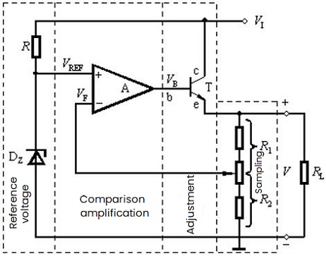
Figure 1: Series Negative Feedback Voltage Stabilization Circuit Block Diagram
The voltage deviation (VREF-VF) is amplified by the op amp, and then controlled by the adjustment tube to control the output. The voltage stabilization process can be briefly described as follows:

If it is under the condition of deep negative feedback, VREF will finally be approximately equal to VF. At this time, the output voltage can be obtained as:

The basic voltage stabilizing principle of the three-terminal voltage regulator is similar to the linear series feedback voltage stabilization circuit. And the output voltage is maintained relatively stable through negative feedback adjustment.
Three-terminal Voltage Regulator Products
7800 Series
Figure 2(a) shows the most basic and simple application circuit of the 7800 series. The parameters of C1 and C2 are all from the data sheet of the 7800 series manual. Most power supply ICs contain op amp, which work the same as high-gain analog amplifiers. They must be installed according to the user manual to avoid oscillation. While capacitors are connected to the circuit to realize frequency compensation. And C1 is an anti-interference capacitor, because the connection oscillation between the filter capacitor and the integrated voltage regulator is likely to occur. This can bypass high frequency interference pulse to make the circuit work stably.
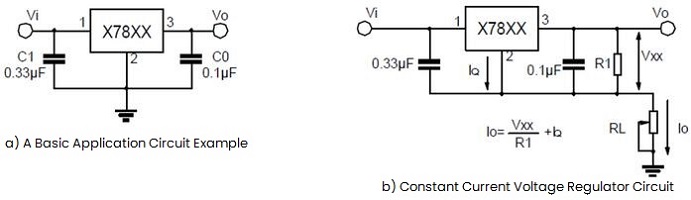
Figure 2: A Basic Application Circuit Example and Constant Current Voltage Regulator Circuit
But in reality, a 10u electrolytic capacitor C3 will be connected to the output end, and a protection diode will be connected between the output and input. The former is to reduce the low-frequency interference introduced by the input power supply at the output end of the regulated power supply; the latter is to protect the voltage regulator. When the input is accidentally short-circuited, it provides a discharge path for C3 to prevent the voltage at both ends of C3 from acting on the emitter junction of the adjustment tube, causing the emitter junction to be broken down and then damage the regulator.
As shown in Figure 2(b), it is a constant current voltage stabilizing circuit with 78XX as the core, and RL is the load resistor. It's easy to get:

Since the voltage regulator's output nominal voltage deviation is very small, the IO has high accuracy and stability.
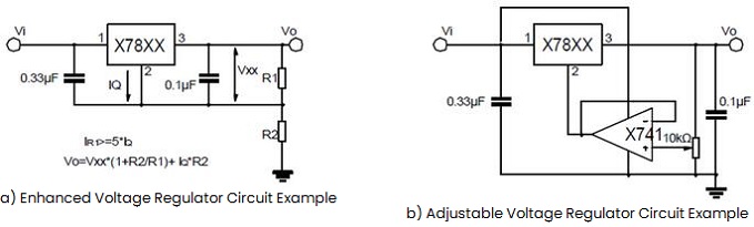
Figure 3: Enhanced Voltage Regulator Circuit Example and Adjustable Voltage Regulator Circuit Example
Shown in Figure 3(a) is an enhanced voltage stabilization circuit with 7800 as the core. In actual application, the voltage value required by the circuit may not be the standard output voltage value of the fixed voltage regulator. In this case, the voltage needs to be appropriately changed before use. It's easy to get:

By appropriately selecting the values of R1 and R2, the desired voltage value can be obtained. However, it is worth noting that when R2 is made larger, the impact of input changes of the voltage regulator on the output will increase. Generally, this circuit is suitable for situations where the voltage is slightly higher than the nominal voltage.
Shown in Figure 3(b) is an adjustable voltage stabilization circuit with 7800 as the core. This circuit uses an integrated op amp to isolate the voltage regulator from the sampling resistor. The circuit uses an op amp for voltage following, and the potential at the slider of the sliding rheostat is the same as pin 2. However, in practical applications, three resistors R1, RP, and R2 are commonly used to replace the sliding rheostat in the circuit, where RP is a sliding rheostat, and R1 and R2 are fixed resistors. The adjustment range at this time:


When designing the circuit, the device can be selected based on the output voltage adjustment range and output current size.
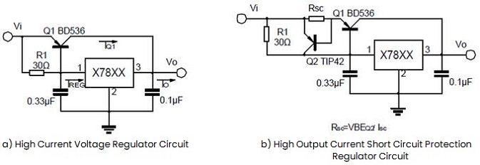
Figure 4: High Current Voltage Regulator Circuit and High Output Current Short Circuit Protection Regulator Circuit
As shown in Figure 4(a), it is a high-current voltage regulator circuit with 7800 as the core, and an external PNP tube is connected and adjusted by the voltage regulator. Here the maximum output current of the 7800 series is 1.5A. When the load current IL is greater than the maximum current, the current can be expanded by connecting an external high-power tube. When IL<=IOM, only 7800 works; when IL>IOM, the excess current is output by the external adjustment tube, where the bias resistance of the external power adjustment tube is determined by the following formula:

Where, UBE is the voltage drop of the emitter junction of the external adjustment tube, and β is the amplification coefficient. The selection of external adjustment tube is determined by the output current and power. Note that if there is a NPN tube, it should be connected to the output end.
In Figure 4(b), it is a high output current short-circuit protection voltage regulator circuit with 7800 as the core. PNP-tube Q2 and current sensing resistor Rsc form an over-current protection circuit, and Q1 is an external adjustment tube. While R1 is used to set the turn-on threshold voltage of Q1. The calculation formula of the main parameters of the circuit is as follows:
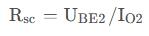
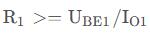
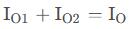
Among them, IO1 is the output current of the voltage regulator, and IO2 is the maximum current that the external adjustment tube can provide. If the output is short-circuited and the output is greater than the maximum output current, the voltage drop on Rsc will be greater than the turn-on voltage drop of Q2, at this time, Q2 is turned on, and Q1 is turned off, thus realizing the overcurrent protection function.
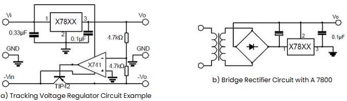
Figure 5: Power Supply Application Circuit Examples
Figure 5(a) shows the application circuit of a tracking regulated power supply composed of a 7800 and an operational amplifier. In some situations where positive and negative power supplies are used, the negative power supply needs to be used to track changes in the positive power supply. Where 7800 is used as the positive power supply, and an operational amplifier and power tube are used to form a traceable negative power supply. In addition, two identical 4.7kΩ resistors are used to control the input potential of the operational amplifier at zero level, and the output terminal is used to control the adjustment tube in the negative power supply loop to maintain the negative output to the positive output.
In Figure 5(b), it is a power application circuit composed of a 7800 positive voltage regulator, a transformer and a bridge rectifier circuit. If you only have a 7800 and want to obtain negative voltage, you can interchange the ground and output terminals, as shown in Figure 6. Further more, the input voltage of the voltage regulator is a relatively stable voltage obtained after rectification and filtering, and if the power supply is commercial power, a transformer is required to step down the voltage.
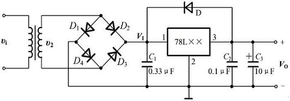
Figure 6: 7800 Series Voltage Regulator Typical Application Circuit
7900 Series
The 7900 series is very similar to the 7800 series in terms of principle and circuit structure. The following will focus on two basic circuits to compare their differences.
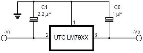
Figure 7: 7900 Series Voltage Regulator Basic Application Circuit
Figure 7 is the most basic and simple circuit in the 7900 series application circuit. Through the circuit, the 7900 outputs a negative voltage, and its circuit connection method is the same as that of the 7800 series. In order to highlight the characteristics of negative voltage, the ground terminal is deliberately placed on it. And the anti-interference capacitor at the input end is 2.2uF according to the 7900 series datasheet, in addition, taking an anti-self-excitation capacitor at the output end is 1uF. The specific functions of these two capacitors are similar to those of the 7800 series.
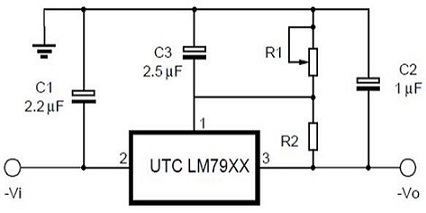
Figure 8: 7900 Series Voltage Regulator Boost Circuit
In Figure 8, the output can be appropriately improved:

R2 is selected according to the relative value of the voltage regulator. For example, LM7905CT uses a 300-ohm resistor, LM7912CT uses a 750-ohm resistor, and LM7915CT uses a 1k ohm resistor. In fact, R2 is a variable resistor. As long as the ratio of the two resistors is changed, different voltage values can be output.
Adjustable Three-terminal Voltage Regulator
Similar to fixed ones, adjustable ones can also be divided into two categories, positive power supply type and negative power supply type. The most commonly used positive power supplies are LM117, LM217, and LM317, and their output voltage range is 1.25-37V. The maximum output current can be judged according to the data manual. While there are three main types of negative power supplies: LM137, LM237 and LM337. For adjustable three-terminal linear voltage regulator, the most commonly used packages are shown in Figure 10.
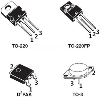
Figure 10: Typical Packages
* Working Principle
Taking LM317 as an example is shown in Figure 11. Its internal circuit mainly consists of a current source circuit, a reference voltage circuit, a comparison error amplifier circuit and a bias circuit, and it is easy to find the relative position of the input, output and common terminals in the diagram.
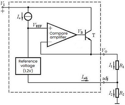
Figure 11: Three Terminal Adjustable Linear Voltage Regulator Block Giagram
In Figure 11, the regulator reference voltage is 1.2V. If the adjustment resistors R1 and R2 are connected externally, due to the characteristics of deep negative feedback, the error comparison amplifier always wants the voltage on R1 to be the same as the reference voltage, then it can be inferred that UR1=VREF. So the output voltage is:

In addition to the value of VO, the functions of R1 and R2 also provide a static current path to ground for the error amplifier and other circuits if there is no load, also known as no-load bias resistor, and meanwhile, it is generally recommended that the current I1 through R1 is 5mA. Where VREF=1.2V of LM317, Iabj=50uA ( it can be ignored). At this time, the output voltage can be approximately expressed as:

In practical applications, VREF often takes 1.25V. In addition, the basic principles of other commonly used adjustable linear voltage regulators are similar to the LM317.
Typical Application Circuits of LM117/ LM217/ LM317
Since the application circuit diagrams of LM117, LM217, and LM317 are all similar, and LM317 is the most commonly used among them, the following circuit diagrams take LM317 as an example.
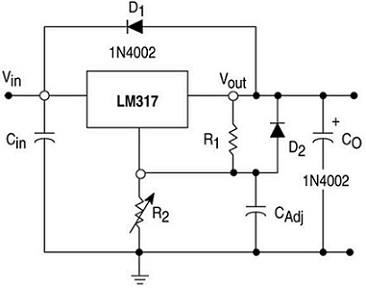
Figure 12: LM317 Adjustable Voltage Output Circuit
The voltage adjustable circuit diagram composed of LM317 is shown in Figure. Among them, R1 and R2 are sampling resistors, and the minimum load current IL of LM317 is 5mA. There are generally two ways to choose the resistance of R1: R1=240Ω, IL=1.25/240≈5mA, and R2=6.8kΩ; R1=120Ω, IL=1.25/240≈10mA, and R2=3.4kΩ. When adjusting R2, a regulated output of 1.25-37V can be obtained. CAdj can filter out the ripple at both ends of R2 so that it cannot be amplified and then output from the Vout end, which is generally 10uF.
D2 is a protection diode. Once a short circuit occurs at the Vin, D1 provides a leakage circuit for CAdj to prevent it from being discharged internally in the LM317. When Vout<7V or Co is small, D2 does not need to be connected. When LM317 is connected to a capacitive load of 500~5000pF, the output end is prone to self-oscillation. For this reason, C1 can be connected to the output end. Generally, a 1uF tantalum capacitor is selected. If an ordinary aluminum shell electrolytic capacitor is used, the capacitance needs to be increased to 22uF. When the output terminal of the linear regulator is connected to the large-capacity load capacitor CL, D1 can play a protective role. Once the input terminal of the linear regulator is short-circuited, the charge accumulated on CL will be discharged to ground through D1. Output voltage calculation formula:

Obviously when R2 is zero, Vout is equal to 1.25V. When R2 is the largest, Vout is equal to 37V. In order to ensure the accuracy of the output voltage, the resistor should be a precision metal film resistor with an error of ±1% or ±0.5%.
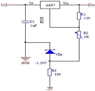
Figure 13: Continuously Adjustable Circuit Example (output voltage 0~30V)
The circuit shown in Figure 14 is a circuit composed of LM317 with a continuously variable output voltage of 0~30V. In order to enable the output voltage to be adjusted from 0V, the lower end of R2 should be connected to a negative potential of -1.25V. This potential can be provided by the voltage regulator VDZ, and VDZ is connected to the -5V power supply through the current limiting resistor R3, in addition, VDZ can also be replaced by two silicon rectifiers connected in series. If the negative power supply voltage is -10V, the resistance value of R3 should be increased to 680Ω.
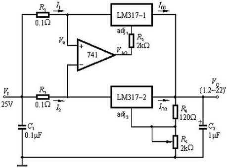
Figure 14: Adjustable Voltage Regulator Circuit with Two LM317s
The maximum output current of LM317 is 1.5A. If you want to get an output current of 3A, as shown in Figure 15, you can achieve an output current of 3A by connecting two LM317s in parallel. The 741 is used to balance the output current of two LM317s, and changing the value of R5 can adjust the output voltage. The input terminals of LM317-1 and LM317-2 are respectively connected in series with 0.1Ω current sampling resistors R1 and R2. When the output current of LM317 increases, IO1↑→UR1↑, add a signal to the non-inverting terminal of 741 to reduce its voltage. In addition, Uadj↓→UO1↓→IO1↓, maintain IO1=IO2. And the converse is also true, the output currents of the two LM317s are always maintained in a balanced state.
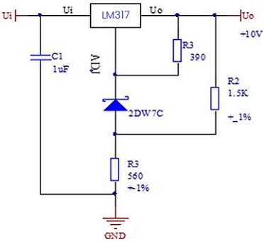
Figure 15: LM317 Linear Voltage Regulator Circuit (High stability, +10V)
The +10V high-stability linear voltage regulator circuit composed of LM317 is shown in Figure 15. Although LM317 has high accuracy, which will be reduced due to the influence of R2 and IADJ. For it, the voltage regulator tube 2DW7C with temperature compensation can be used to replace R2. The stable voltage UZ of 2DW7C is 6.3V, if UZ

Taking UZ=6.3V, R3=560Ω and R2=1.5kΩ into the above formula, we can get UO=10.3V
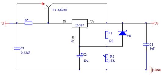
Figure 16: Circuit for Expanding the Output Current by Connecting an External PNP Power Tube
As mentioned earlier, multiple LM317s can be connected in parallel to achieve current expansion. Of course, power tubes can also do it. As shown in Figure 16, an external PNP tube is connected to the circuit to expand the output current. Due to the limitations of the internal circuit of LM317, if a power tube is added to the input end, it is suitable for PNP and cannot use NPN tube directly. LM317 adopts emitter output mode, and the power tube provides the part beyond the original output current. When the output current I≤IO, only LM317 works; when the output current I>IO, LM317 and the external adjustment tube work together. After expanding the output current, the output current I=IO+IC.
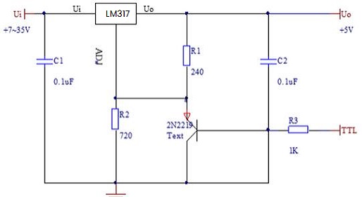
Figure 17: A Voltage Regulator Circuit Example Controlled by TTL Level
Sometimes we may need a circuit whose output can be controlled. The reality of such a circuit often uses electronic switches, which can be a transistor. A linear regulator controlled by TTL levels is shown in Figure 17. The input voltage range of this linear regulator is 7~35V. And the output voltage is controlled by the TTL level: when the input is high, 2N2219 is turned on, R2 is short-circuited, and the output voltage UO is 1.25V; when the input is low, the output voltage is:

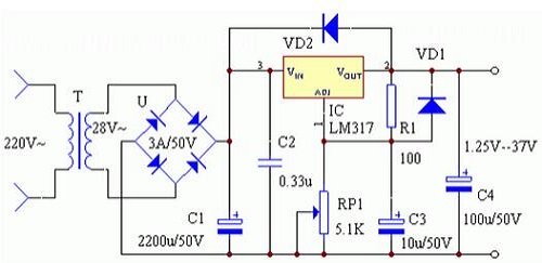
Figure 18: LM317 Voltage Regulator with Step-down Rectifier Filter Circuit
Typical Application Circuits of LM137/ LM237/ LM337
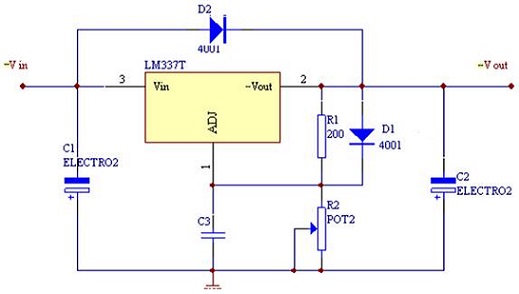
Figure 19: LM337 Adjustable Voltage Output Circuit
For LM337, it is necessary to remember the reference voltage, that is, the voltage between the output terminal and ADJ is -1.25V. We can achieve a continuously variable output voltage of -1.25~-37V by adding an external sampling resistor. Because of the negative voltage, the two protection diodes are in the opposite direction to the previous one. To ensure the output performance of the voltage regulator, R1 should be less than 240Ω(I>5mA). Normally the LM337 does not require external capacitors unless some special situations.
Here R1 and R2 in Figure 20 should use precision metal film resistors with an error of ±1%, and LM129A is a 6.9V precision reference voltage source.
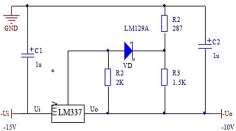
Figure 20: LM337 Linear Voltage Regulator Circuit (High stability, -10V)
Using LM317 (positive voltage output) and LM337 (negative voltage output), a positive and negative adjustable linear voltage regulator can be formed, as shown in Figure 21.
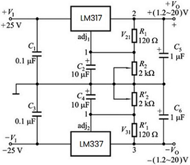
Figure 21: LM317 Linear Voltage Regulator Circuit (High stability, -10V)

 English










