It is reported that Apple's 3D chip stacking technology SoIC will be used in MacBook, and end products will come out as soon as 2025. What’s more, AMD will be the first customer, and its latest MI300 APU uses SoIC with CoWoS. So what is the magic of SoIC? In simple terms, it is a new type of IC packaging technology that can stack multiple chips together to achieve higher integration with smaller size.
For consumers, this revolutionary MacBook will also bring more choices. With the development of 3D stacking technology, we can see that more electronic products will adopt it, from mobile phones, tablets to TVs, cars, and even home smart devices, will benefit from the innovation brought by it.
Why Does 3D Stacking Technology Appear?
The functions of modern chips are becoming more powerful, resulting in more complex process technologies, which brings design and manufacturing cost issues. In order to solve them, many people have thought of the method of using modular design, that is, separating the functional blocks into small modules to make core particles with high yield, low cost and different functions, and then flexibly assemble them according to needs.
In recent years, research and development of core particles have been carried out in academia and industry. Chips can generally be assembled or stacked through an interposer in a 2.5-dimensional architecture. This technology refers to connecting multiple chips on a silicon interposer with interconnect lines. Since the interconnect density on a silicon substrate can be much higher than that on a traditional PCB, high-level integration can be made. For example, CoWoS and InFO launched by TSMC, Intel's EMIB and other technologies.
The traditional 3DIC technology is to stack multiple chips together and use TSV technology to interconnect different chips. At present, 3DIC is mainly used in the stacking structure between memory chips and sensors, while 2.5DIC has been widely used in a variety of high-end chipsets. In addition, 3D and 2.5D are not completely opposite. For example, in HBM memory, 3DIC is used to integrate multiple memory blocks, while 2.5DIC is used to integrate memories and main chips.
At present, seizing the opportunities offered by advanced 3D integration packaging technology, chips are opening new ways for safe and reliable electronic system design. By adjusting the number of chips placed in a chip package, systems of different scales can be created, which greatly improves the flexibility and scalability of the design, and also greatly reduces the R&D cycle and cost.
What is 3D Stacking Technology?
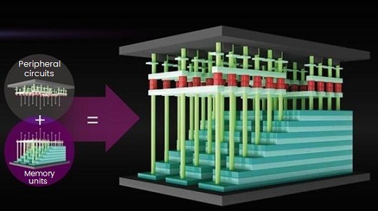
From the birth of the world's first CPU to today, even including Moore's Law itself, they all belongs to two-dimensional level. That is to say, the research focuses on how to increase the number of components per unit area and improve the microscopic precision. The concept of 3D stacking is a new way to break the usual. So what is 3D stacking technique?
The CPU is an ultra-large-scale integrated circuit board, and millions of transistors are placed on it, and there is no longer any blank space. Why not put a board on top of it? 3D stacking results from this.
3D stacking technology is the formation of 3DIC in the Z-axis direction of chips or structures through interconnection and other micro-processing technologies, while signal connections, and wafer-level, chip-level and silicon lid packagings with different functions. It is used for microsystem integration and is an advanced system-in-package manufacturing technology developed after system-on-chip (SoC) and multi-chip module (MCM).
In short, the so-called 3D stacking technology is to package two or more chips in the vertical direction with different functions in the original package, generally without changing the size of the original package. This will naturally realize the diversification of chip functions in a three-dimensional model.
In a traditional SiP packaging system, any stack of chips can be called 3D because of the expansion of functions and signals in the Z axis, whether inside or outside the IC.
Generally speaking, 3D stacking technology has more advantages in terms of integration, performance, and power consumption. At the same time, it has a higher degree of design freedom and shorter development time. With the rise of applications such as high-performance computing and artificial intelligence (AI), and the maturity of TSV technology for providing multi-wafer vertical communication, we can see that more and more CPUs, GPUs and memories are beginning to use it.
Three Examples of 3D Stacking Technology
1. AMD's Zen 3
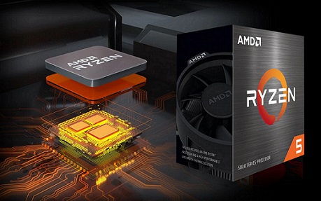
AMD's 3D V-Cache technology connects a 64-megabyte SRAM cache and two blank structure chiplets to the Zen 3 computing chiplet.
PCs have long offered the option to add more memory to provide faster speeds for very large applications and data-heavy work. AMD's new CPU chiplets also offer that option, thanks to advances in 3D stacking technology. Both the Zen 2 and the new Zen 3 processor cores use the same TSMC manufacturing process - so they have the same size transistors, interconnects and everything else. AMD made so many architectural changes that they were able to achieve a 19% performance boost in Zen 3 even without the extra cache. One of the typical features is the inclusion of through-silicon via (TSV), vertical interconnects that run directly through most of the silicon, and it built into Zen 3's highest level of cache - the SRAM block called L3.
For data-heavy processors, the backside of the Zen 3 wafer is thinned until the TSVs are exposed. Then an SRAM chiplet is bonded to those exposed TSVs using so-called hybrid bonding, a process similar to cold soldering copper together, so that a dense set of connections can be as tight as 9 microns. Finally, for structural stability and heat conduction, a blank silicon die is attached to cover the rest of the Zen 3 CPU die.
Adding extra memory by placing it next to the CPU chip is not an option because the data takes a long time to reach the processor core. Despite quadrupling the L3 size, only four clock cycles of latency have added to the the 3D V-Cache, achieved by 3D stacking” said John Wuu, AMD senior fellow design engineer.
Larger caches have their place in high-end gaming. For example, gaming at 1080p is 15% faster on average with a desktop Ryzen CPU and 3D V-Cache. It's also suitable for more professional work, cutting the runtime of difficult semiconductor design calculations by 66%.
Wuu also noted that the industry's ability to shrink SRAM size is slowing down compared to shrink logic. But it can still be expected that future SRAM expansion packs will continue to be manufactured using more mature processes, while computing chips are pushed to the forefront of Moore's Law.
2. Graphcore’s Bow IPU Processor
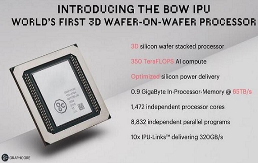
The Bow IPU processor uses 3D chip stacking to boost performance by 40%. 3D integration can speed up calculations even without a single transistor on one chip in the stack. Graphcore has dramatically increased the performance of its systems simply by putting power-supplying chips on top of its processors. Adding power supply silicon means its combo chip can run faster (1.85 GHz compared to 1.35 GHz) at a lower voltage than its predecessor, and consume 16% less energy than the previous generation. Further more, users do not need to change their software to receive this improvement.
The power management chip is composed of capacitors and through-silicon vias. The latter simply provides power and data to the processor chip, and capacitors really play a big role. Like the bit-storage components in DRAM, these capacitors are formed in deep, narrow trenches in the silicon. Because they are so close to the processor's transistors, power delivery is smoothed out, allowing the processor core to run faster at lower voltages. Without a power chip, the processor would have to boost its operating voltage above its nominal level to operate at 1.85 GHz, but consume more power. With a power chip, it can also hit that clock rate and consume less power.
The manufacturing process used to make the BoW is unique, but it's unlikely to stay that way. Most 3D stacking is done by gluing one chiplet onto another while one is still on the wafer, known as chip-on-wafer. But Bow used TSMC's wafer-to-wafer, in which an entire wafer of one type is bonded to an entire wafer of another type, then has dicing. Graphcore chief technology officer Simon Knowles said it was the first chip on the market to use this technology, which enables a higher density of connections between two die than can be achieved using a chip-on-wafer process. Although power chiplets don't have transistors. This is the first step, and it will play a greater role in the future.
3. Intel's Ponte Vecchio
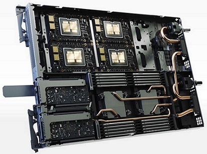
The Aurora supercomputer aims to be one of the first high-performance computing (HPC) in the U.S to break the exaflop barrier -- one billion high-precision floating-point calculations per second. To get Aurora to those heights, Ponte Vecchio packs more than 100 billion transistors from 47 silicon chips into a single processor. Intel uses both 2.5D and 3D technologies to squeeze 3,100 square millimeters of silicon (nearly equal to four Nvidia A100 GPUs) into a 2,330 square millimeter footprint. It is the limit of such a integration technology.
Each Ponte Vecchio is two mirrored chiplets bundled together using Intel's 2.5D integration technology Co-EMIB, which forms a high-density interconnect bridge between two stacks of 3D chiplets. The bridge itself is a small piece of silicon embedded in a packaged organic substrate, where the density of interconnect lines can be twice as high as on the organic substrate. The Co-EMIB die also connects the high-bandwidth memory and I/O chiplets to the "foundation block," which is the largest chiplet in the rest of the stack.
The base tile uses Intel's 3D stacking technology, called Foveros, to stack compute and cache chiplets on top of it. The technology creates a dense array of chip-to-chip vertical connections between two chips. These connections can be 36 microns, except for short copper pillars and solder microbumps. Signals and power enter this stack through silicon vias, fairly wide vertical interconnects that go right through most of the silicon. 8 compute tiles, 4 cache tiles, and 8 blank "hot" tiles for cooling from the processor are all connected to the base tile, and the base itself provides cache memory and networking that allows any compute block to access any memory.
It innovates in yield management, clocking circuitry, thermal regulation and power delivery. For example, Intel engineers chose to supply the processor with a higher than normal voltage (1.8V) so that the current was low enough to simplify packaging. Circuitry in the base block steps down the voltage to nearly 0.7V for the compute blocks, and each block must have its own power domain in the base one. The key to this capability is a new type of high-efficiency inductor called a coaxial magnetically integrated inductor. Because these are built into the package substrate, the circuit actually winds back and forth between the base block and the package before supplying voltage to the compute block.
Technical Bottleneck
Since this 3DIC stacks different materials, the expansion rate of the material is different, and uneven internal stress may appear when it is affected by high temperature during processing, resulting in problems such as warping, cracking, and collapse, which increases the difficulty of the etched through hole. In a chip, billions of holes need to be etched, so the yield rate problem is a very big challenge.
Facing the severe pressure of drilling, it is necessary to continuously improve the etching process, develop more suitable chemicals (for etching, cleaning), find more matching materials, and gradually reduce the thickness of each layer, the time of deposition, etching, cleaning, the thermal stress, etc.
Stacking also brings thickness issue. If the number of stacked layers doubles, the thickness of the bare die will gradually increase, which is not a good thing from the perspective of packaging. Fortunately, with the development of 3D NAND Flash so far, the thickness increase of the bare die is not linearly related to the number of layers. And the thickness of each layer is gradually reduced, which can be reduced by about 10% every one to two generations. The layer of early 3D NAND is about 70nm, and the stack thickness of memory cells is about 2.5μm. In late period, the layer thickness is reduced to about 50nm, and the stack thickness is about 7~10μm. With the peripheral control circuit, power layer, and silicon substrate, the thickness of the bare die is about 50μm. If 16 dies are stacked, the thickness is close to 1mm, after packaging, it is roughly 1.5~2mm.

If this variation is counteracted by the thin silicon substrate (to keep the package thickness the same as the existing level), the challenge of the mechanical strength of the substrate is still very large. When the layer thickness is reduced to less than 35nm, the thickness of the gate in the vertical direction will also be reduced to less than 20nm. The problems of crosstalk and wear between the gate and the insulating layer (horizontal direction) encountered at the end of 2D NAND will also occur in 3D. So 3DIC stacking tech has a long way to go.

 English










