In the module, the parallel connection of the devices is very simple: two chips are mounted side by side and the remaining nodes are connected by short bonding wires. The alignment is shorter and the thermal coupling is better.
Thermal coupling between discrete devices is not as good as in modules. Heat travels from the chip to the package, through the thermally conductive interface material (TIM) to the heat sink, and on to the other MOSFETs. each medium, and each transition between them, creates a thermal resistance that results in a temperature gradient.
Motivation for parallel discrete MOSFETs
Despite these limitations, paralleling discrete MOSFETs offers irreplaceable advantages: design flexibility, parametric scalability, supply chain redundancy, and ease of prototyping. In addition, paralleling itself offers the following physical optimisations:
Thermal resistance is inversely proportional to package heat sink area. When losses are split evenly between two identical devices, the total heat sink area is doubled and the heat dissipation of a single package is halved, thus halving the junction-to-heatsink thermal resistance and bringing the actual device temperature closer to the heat sink temperature.
MOSFET losses mainly contain conduction losses and switching losses. The conduction loss is caused by the channel on-resistance (RDSon), and connecting N identical MOSFETs in parallel can reduce the total RDSon to 1/N.
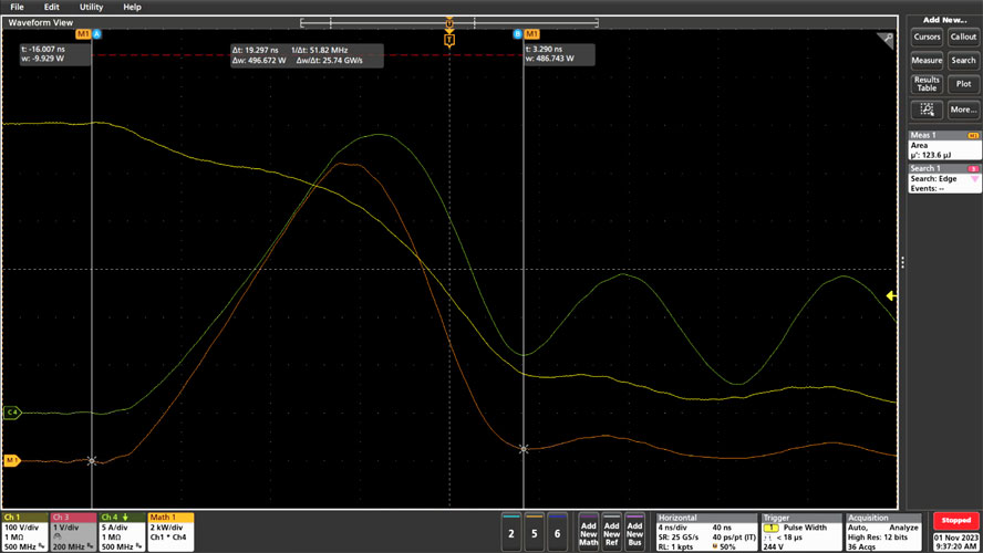
Fig. 1 Conduction example: Ch1 drain-source voltage, Ch4 drain current, Math power dissipation
Switching losses arise from the overlap of voltage and current during switching (Figure 1). Despite the very short transient times, the peak power at high voltage and high current is very significant. The switching losses can be calculated by integrating the power over time (the area below the curve) to obtain the turn-on and turn-off energies for a given condition, and multiplying the two by the switching frequency (or accumulating all the energies over 1 second if the condition changes).
The given conditions are the place to pay attention to, since the switching energy depends strongly on several parameters: transient time, voltage, current and temperature. Regarding the parallel scheme, there are some advantages hidden in the current function of the switching energy. (Fig. 2)
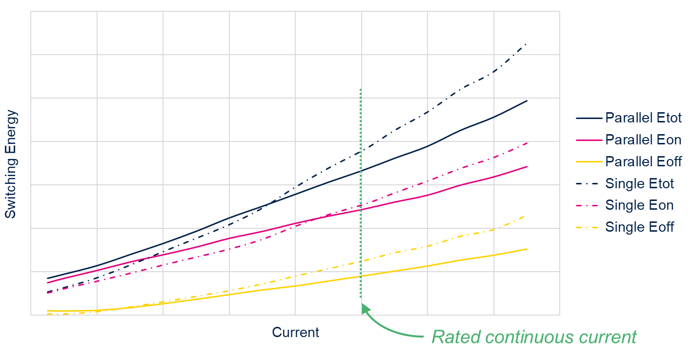
Fig. 2 Example of switching energies: single MOSFET and two in parallel
The curve of change in switching energy is not linear and has a slightly exponential trend. Doubling the current therefore results in more than a twofold increase in energy. In parallel, the result is the opposite: if the current is divided equally between two identical devices, the total switching energy is lower than if the individual devices were switched separately.
If we compare a single MOSFET in a power module with two discrete MOSFETs, the module will be at a disadvantage:
Comparing a single MOSFET in a power module with two MOSFETs in discrete form, the module is instead at a disadvantage:
-
Heat dissipation path: Due to the different structure of the module, it is difficult to compare the heat dissipation path, however, discrete devices can make up for the structural disadvantage through a larger heat dissipation area, and even exceed the performance of the module.
-
Conduction loss and switching loss: the conduction loss of discrete MOSFETs in parallel is one-half of that of power modules, and the switching energy loss is significantly reduced, so the advantage of parallel discrete MOSFETs in terms of loss is very obvious.
This suggests that there is an overlap in performance between the parallel connection of discrete devices and the modular solution over the stated power range. Using more devices of the same specification can increase the power, while choosing higher on-resistance at lower cost when paralleling may still be able to compete with the module scheme at the same power.
Thermal runaway - the pitfalls behind the advantages
The on-resistance (RDSon) of a MOSFET is not a static parameter; its value varies with current and is more significantly affected by temperature. In the current power range, silicon carbide (SiC) MOSFETs have become the mainstream choice, with RDSon temperature characteristics far superior to those of silicon-based MOSFETs.
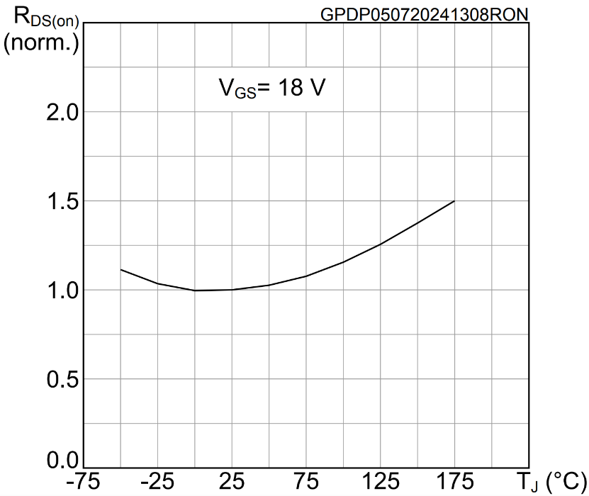
Fig. 3 On-resistance versus temperature normalised curve for SCT011HU75G3AG
In the case of the SCT011HU75G3AG in ST's latest-generation HU3PAK package (top-side heat sink) (Figure 3), for example, the on-resistance RDSon is very low, making it ideal for parallel designs.
However, from 25°C to 175°C its on-resistance RDSon rises by only about 50 per cent, a significantly lower increase compared to standard silicon-based MOSFETs, which can increase by up to 200 per cent at 150°C (rather than 175°C, which is their absolute maximum temperature rating).
A flat on-resistance (RDS(on)) temperature profile is an ideal design characteristic that keeps on-state losses stable over temperature. However, when losses rise, there is a risk of thermal runaway: increased losses lead to higher temperatures, which in turn further exacerbate losses. This positive feedback effect, once a problem with silicon-based MOSFETs, is usually negligible with silicon carbide (SiC) devices - unless a parallel configuration is used.
Why the difference? The key lies in parameter dispersion, especially on-resistance RDS(on). Model SCT011HU75G3AG, for example, has a nominal RDS(on) of 11.4 mΩ, but in reality it could be as high as 15 mΩ. Although the probability of such a large deviation within the same batch is low, let's analyse this as an extreme case: 15 mΩ is 32% higher than 11.4 mΩ, which means that the device will carry 32% less current at the same voltage. As a result, an 11.4 mΩ MOSFET will have about 32% more losses and will be more prone to heating. If the slope of the RDS(on) rise with temperature is greater, although it will result in higher losses, the MOSFET that heats up more will shift current to the lower temperature device by self-regulating (warming up causes resistance to increase).
Practical application analysis
What is the risk level in practical applications? Due to the fact that parallel MOSFETs share the heat sink (thermal coupling exists), this still poses a serious threat. In order to verify this issue, we perform an in-depth study through simulation: assume two SCT011xx75 MOSFETs in HU3PAK package (TO247 package would perform better, the more severe case is chosen here), one with RDS(on) = 11.4 mΩ, the other = 15 mΩ. The heat sink temperature is set to 90°C, and the thermally conductive interface material (TIM) is used as a gap-filling adhesive (thermal conductivity 7 W/(m-K), thickness 0.4 mm). The focus is on conduction loss at a total RMS current of 140 A. The cooling area of the HU3PAK is 120 mm2 , and the shell-to-heatsink thermal resistance due to TIM is calculated to be 0.476 K/W.
Simulation Experiment Results
-
63 A of the 140 A current flows through the 15 mΩ MOSFET, with a case temperature of 123.7°C and a junction temperature of 139.9°C
-
The remaining 77 A flows through the 11.4 mΩ MOSFET, with a case temperature of 131.8°C and a junction temperature of 151.8°C
The current dissipation is 22% compared to the initial value of 32% and both MOSFETs have ample temperature margins, i.e., the difference between the actual temperature and the maximum absolute temperature is large. the thermal gradient of the TIM thermal compound is a key factor, with a temperature drop of 33.7°C from the case to the heat sink in the 15 mΩ MOSFET, compared to 41.8°C in the other MOSFET. In this case, the TIM thermal conductivity adhesive is the real limiting factor and the current imbalance between the MOSFETs is not an issue. Thermal conductivity was chosen to be 7 W/(m∙K), which is a good value, but not optimal. Fortunately, recent market demand has fuelled research into such materials, and galvanic isolation gap fillers in excess of 20 W/(m∙K) are now available.
Reach a verdict
Power modules are suitable for high power application scenarios, but discrete MOSFETs also offer a number of advantages that make them equally suitable for the power range of the module. What are the key factors to consider when choosing the right MOSFET? The answer is excellent switching performance and outstanding thermal management.
Fortunately, ST's third-generation SiC MOSFETs have been developed to maintain stable switching performance when connected in parallel, and their thermally variable on-resistance, RDSon, is optimised for both reduced energy loss and effective suppression of thermal runaway.

 English










