In electrical circuits, parasitic capacitance is an unavoidable and unwanted capacitance that exists between the parts of an electronic component or circuit. Common components such as inductors, diodes, and transistors all have internal capacitance that will cause the device's performance to differ from ideal conditions, especially at high frequencies. Therefore, it is necessary to take care of PCB design.
Parasitic Capacitance
Parasitic Capacitance in PCB Layout
Parasitic capacitance is a virtual capacitance that exists between two conductive structures separated by an insulator. It is an additive effect in the PCB layout, where the propagated signal behaves as if it is a capacitance, but not real.
In PCB, parasitic capacitance can appear basically anywhere. You can refer to the layout below, which marks the area where the capacitance protrudes the top layer, of course other layers may also exist.
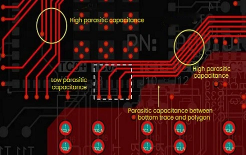
Figure 1: Parasitic Capacitance in PCB Layout
What Are the Influences of Parasitic Capacitance?
1) Has band-limited behavior in transmission lines, and produces low-pass filter behavior at very high frequencies.
2) Causes noise coupling between grounds with different potentials, then results in common mode noise.
3) Making noise or signals are coupled into components, especially high-frequency capacitive crosstalk of wire-wound inductors (manifested as FEXT and NEXT).
4) Make PDN impedance modification due to spacing between power and ground planes.
5) Causing EMI couples into the heat sink, which generates common mode current.
Figure 2 shows a simple example of how parasitic capacitance arises in PCB layout. Here, there is an arrangement of conductors separated by insulators, forming a complex structure with an equivalent capacitance. This example can be modeled as an arrangement of capacitors, but note some parasitic inductance and resistance in the structure. It is this equivalent capacitance and inductance that determines the impedance in a PCB layout.
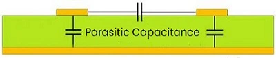
Figure 2: PCB Parasitic Capacitance Example
Parasitic Capacitance Calculation and Reduction
How to Calculate Parasitic Capacitance?
Figure 3 shows the charge and discharge cycle of the capacitor.
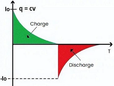
Figure 3: Capacitor Charge and Discharge Cycle
It's impossible to avoid parasitic capacitance a conductor and is the amount of storage per unit potential change. The related calculation formula is:
C=q/v
C: Capacitance, unit: Farad (F)
V: voltage, unit: volt (V)
Q: Charge, unit: Coulomb (C)
1) For a constant electrical signal that does not change with time, dv/dt = 0, that is, the potential does not change: i=0
2) If there is a capacitor in the circuit loop, dv/dt will converge to a fixed value, the potential will change, and a current will be generated: i≠0
How to Calculate Trace Capacitance?
The capacitance of the parallel plate capacitor is: C=(kA/11.3d)pF
C: Capacitance
A: Plate area
k: Relative dielectric constant of the plate material
d: Distance between plates
The calculation diagram for trace capacitance is as follows:
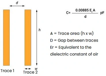
Figure 4: Calculation Diagram of Trace Capacitance
How to Suppress Parasitic Capacitance?
It is impossible to completely eliminate parasitic capacitance in the actual use of PCB, but it can be reduced or limited its impact on signal and power integrity. Here are 10 measures:
1. Avoid parallel wiring.
When parallel wiring is used, the area between metals is the largest and the parasitic capacitance is also the largest.
2. Remove the power layer.
The power plane is generally considered the AC ground and is identical to the ground plane, so removing the power plane is just as important as removing the ground plane near the conductors.
3. Use Faraday shield or protective ring.
Place one of them between the two traces to minimize parasitic capacitance effects.
4. Keep key traces as narrow and short as possible.
To minimize parasitic capacitance, make critical traces as narrow as possible so that the PCB process can handle them, maintaining a good distance from nearby traces.
5. Avoid overuse of vias.
Excessive use of vias will increase parasitic capacitance. It is best to use patches instead of vias as much as possible.
6. Avoid component separation.
Correct wiring between components, power and ground planes, outputs and inputs, etc., is very important to reduce unwanted parasitic capacitance.
7. The signal layer should be sandwiched between two ground layers or between a ground layer or a power layer.
For example, in a 4-layer board, you can put the power layer on the bottom layer and route some sensitive traces between the power layer and the ground layer, which can prevent EMI from signals in one layer from signals in another layer causing noise.
8. Determine the appropriate layer thickness.
Thinner layers can reduce loop area and parasitic inductance, but increase parasitic capacitance.
9. Signal integrity
The key is reducing impedance, usually due to higher return loss due to impedance mismatch between interconnects and driver/receiver components due to proximity of grounded copper traces in the layout, and high pass filtering behavior results in higher insertion loss. The simple solution is to increase the distance between the interconnect and any conductors that are not the required reference plane.
When designing, careful consideration should be given to trace widths on the PCB, nearby conductors, nearby copper pours, and creating coplanar trace arrangements, where copper pour issues are common to the signal integrity issues mentioned above.
So PCB Layout should take the time to calculate the minimum clearance required between the copper and its traces to ensure impedance control. Figure 5 shows example calculations for an Isola 370HR laminate with 50Ω CPW microstrip and stripline.
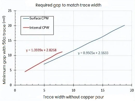
Figure 5: Parasitic capacitances between two microstrips and between them and nearby ground planes.
10. Power integrity
Parasitic capacitance is not completely bad in terms of power integrity, and can be compared to a PDN structure in a circuit board involving multiple ground systems. A common situation where it is undesirable is in systems with multiple ground points, such as PCB power ground planes, system ground areas, and chassis grounds. However, in these systems, especially in high-current power supplies, it may exist between the PCB ground plane and the chassis ground, allowing common-mode current to pass through the system.
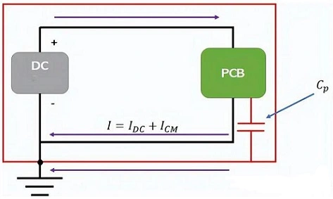
Figure 6: Parasitic Capacitance of Equipment Chassis
Figure 6 shows how the parasitic capacitance of the equipment chassis creates a path for common-mode current flow when the PCB ground plane and chassis ground are at slightly different potentials.
Example of Reducing PCB Parasitic Capacitance
1. High dV/dt Nodes in Switching Regulators
The voltage regulator example section below illustrates the location of the strong dV/dt node and why this layout will have greater coupling to its feedback loop than to any nearby parts of the system. This node has some parasitic capacitance to the nearby ground area, and if there are some other components or circuits nearby, the parasitic capacitance of these circuits will cause switching noise in those circuits. A nearby ground helps some, but what really prevents noise coupling is the capacitor from SW_OUT back to the regulator chip, which provides a low impedance path for high dV/dt switching noise back to the high side of the switching stage, effectively decoupling the switching stage output is decoupled from GND.
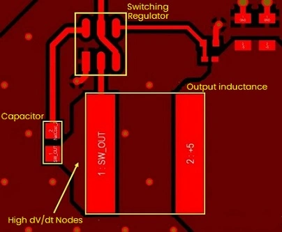
Figure 7: High dV dt Nodes in Switching Regulators
The dV/dt node may be responsible for noise coupling around the PCB layout, and intentionally placed capacitors can prevent this from happening. Another way that can help reduce parasitic capacitance between SW_OUT and nearby traces or circuits is to utilize the GND plane of the next layer. Placing the GND plane closer to high dV/dt nodes will reduce mutual capacitance by creating a stronger electric field coupling to GND compared to coupling to other nodes in the PCB layout.
2. Mutual Capacitance Between Two Traces
Capacitive crosstalk is one of two types of coupling between traces (the other is inductance) where a signal on one trace creates noise on the other, while at progressively higher frequencies, this is dominated by mutual capacitance. Here are two options to reduce parasitic capacitance:
1) Bring the ground closer to the trace while making the trace narrower (fixed impedance target)
2) Increase the spacing between traces
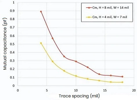
Figure 8: Simulation results show how the parasitic capacitance between two 50Ω traces is affected by the distance from the GND plane (denoted H).
3. Use Diodes to Reduce Parasitic Capacitance.
On high-speed signal lines, some additional functions are usually added. These functions usually have adverse effects, such as generating large parasitic capacitance, which depends on the specific circuit module. If ignored, it may affect the frequency of this signal. The most unfortunate thing is that even if you notice this capacitance, it seems that there is nothing you can do because it is too large generated by the additional functional modules. The common accessory function access method is shown in Figure 9:
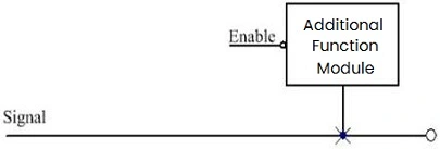
Figure 9: Universal Accessory Function Access
In order to reduce the parasitic capacitance on the signal line, you can add a diode at the access point of the accessory function. This diode must have a relatively small capacitance, because a small signal switch tube is generally used. If the problem of large current is considered, you need to carefully consider the selection.
The forward access method is as shown in Figure 10. The diode is connected between the signal line and the accessory function module, which means that the additional function module outputs a high level when enabled. In addition, in order to reduce the parasitic capacitance to a greater extent, the diode is usually operated in a reverse biased state, that is, UL is connected to a low level. When the additional function module is not working, the diode is under the maximum reverse bias voltage and has a smaller node capacitance, so the signal line can work at high frequency, making the system obtains higher performance.
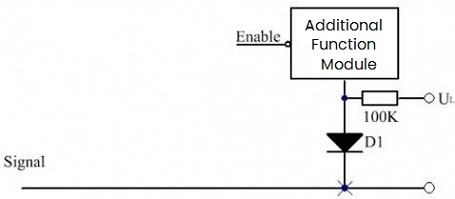
Figure 10: Forward Access
The reverse access method is shown in Figure 11. Different from the forward access, the anode of the diode is connected to the signal line and UH is connected to high level.
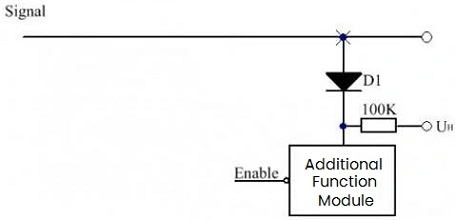
Figure 11: Reverse Access
Regardless of the forward or reverse access method, the equivalent circuit is shown in Figure 12. We assume that the junction capacitance of the diode is 3pF and the total parasitic capacitance of the accessory functional module is 1uF (if the resistance is large enough, it can be ignored). At this time, two capacitors are connected in series, similar to the parallel connection of resistors, CT=C1*C2/(C1+C2)≈C1 (C2 is larger), even if the large capacitance changes greatly, the total series capacitance is almost equal to the small capacitance (3pF), which effectively reduces the access capacitance.
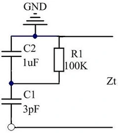
Figure 12: The Equivalent Circuit
The above working principle is based on the unidirectional conductivity of the diode and the small capacitance. Of course, forward access and reverse access cannot solve all situations, that is to say, they can only target special functional modules. In short, it is necessary to have detailed analysis of specific issues.

 English










