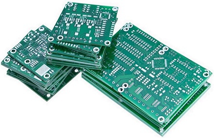
A printed circuit board, or PC board, or PCB, is a non-conductive material with conductive lines printed or etched used to mechanically support and electrically connect electronic components. So how much do you know about PCB design rules?
PCB Design Basic Steps
1. Terminology
Basic Parts
The PCB base material is composed of a dielectric layer (insulating material) and a high-purity conductor (copper foil). The most commonly used one is copper-clad epoxy fiberglass cloth laminate, also called FR-4 all-glass Fiberboard, laminated with fiberglass cloth impregnated with epoxy resin.
1) Network: Circuit is also called network.
2) Board frame: Before placing the PCB package, you need to draw the PCB board frame on the corresponding layer.
3) Jumper wires: It is an electric wire that connects remote electric circuits used for printed circuit boards, and it should be placed on the component side of the circuit board assembly when possible.
4) Soldering pads: They are used to fix and connect electronic components to the PCB. Each pad has an independent number to facilitate correspondence with the component pins.
5) Teardrop: Smoothly transition the connection between the wiring and the pad, improve the reliability of the connection, reduce the sharp jump of impedance during signal transmission, and avoid the reflection of high-frequency signals due to the sudden reduction of line width.
6) Copper laying: It refers to reserve the entire copper foil area for connecting to ground or power supply. A PCB can be set up and drawn with multiple copper laying areas separately.
Wiring
1) Differential pair wiring: This is an effective high-speed signal wiring method that can suppress common-mode noise and achieve better signal integrity, while equal length and equal distance are the most basic requirements for differential wiring.
2) Serpentine routing: It is used to solve the difference in arrival time of parallel signals caused by unequal line lengths under high-speed signals, which will change signal timing. And it has no so-called filtering or anti-interference capabilities, so it is only applicable to timing match.
PCB Cutting
1) Splicing: It is used to make full use of PCB boards and place multiple pieces on one, thereby improving production efficiency.
2) V cut: It means that the board factory uses a cutting machine to open a V-shaped groove in a specific position of PCBs in advance according to requirements. And the distance between the PCB trace and the V-cut line should not be less than 0.4mm to avoid damage.
3) Stamp hole: It is to make some small holes on the board for the convenience of later board splicing. Since it is easy to cause problems such as burrs, it is only used for irregular boards.
4) Half hole: It is usually used to make core board pins, that is, via holes that are accurately cut into half.
Via Hole
1. Basic
Vias are copper-plated metal holes used to achieve electrical connections between different copper layers. They can be divided into the following three types:
1) Through: Connects the top layer and the bottom layer that runs through the entire PCB.
2) Blind: One end is located on the surface of the PCB and the other end is located on the working layer in the middle of the PCB.
3) Buried: It is the connection between the two middle working layers inside the PCB.
Note: For the sake of signal integrity, the use of vias should be reduced, especially Blind and Buried vias must be used, which not only increase the difficulty of PCB processing, but also bring lots of electrical safety issues.
2. Parasitic Capacitance
The via itself has a parasitic capacitance to ground, which will prolong the rise time of the transmission signal. For example, for a PCB board with a thickness of 50 mil, for a via with a diameter of 20 mil and an inner diameter of 10 mil, and its distance from copper area is 32mil, the parasitic capacitance of the via is about 0.5pF.
Although the parasitic capacitance of a single via hole does not significantly slow down the rising edge of the signal, if the via hole is used multiple times for inter-layer switching during the wiring process, the influence of it will rise linearly.
3. Parasitic Inductance
In addition to the above, there are also parasitic inductances. In high-speed digital circuits, the damage caused by the parasitic inductance of the via holes is often greater than that of the parasitic capacitance. The series parasitic inductance generated by multiple via holes will weaken the function of bypass capacitor, thereby reducing the filtering effect of the entire power system. Further more, when connecting the power layer and the ground layer, it often needs to use two vias, which will double the parasitic inductance, so you need to pay extra attention when using bypass capacitor.
Solder Mask
Solder mask refers to the part of the PCB that needs to be covered with solder mask ink. The solder mask layer is usually output using a negative film, so after it is mapped to the PCB, it is not filled with solder mask ink, but to expose the copper foil.
Solder Mask Bridge
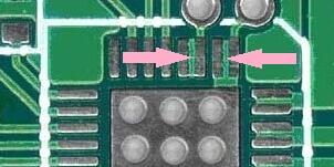
It is the solder mask between chip components (the width of the solder mask ink is reserved between the two solder mask openings, usually greater than 6 mil). It is mainly used to prevent the solder pad from short-circuiting to the tin during soldering.
Solder Mask Opening
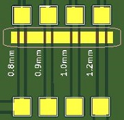
This refers to the part of the copper clad board that is not covered with ink, that is, the copper plating part of the PCB surface is exposed.
Wrapping
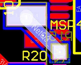
This refers to using a grounding network to wrap the signal lines to reduce crosstalk.
Fan-out
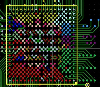
Fan-out design is a work after the PCB layout is completed and before wiring. The purpose is to connect the SMD component pads that only exist on the surface layer to the inner layer of the PCB through a section of traces and vias, so that when the inner layer wiring is performed later, you don’t need to pay attention to the SMD component pads on the surface layer. You only need to connect the vias after the Fanout.
Units Conversion
Mil is a unit of length often used in PCB design. It represents one thousandth of an inch and its conversion method is as follows:
|
1 mm → 39.37 mil
|
|
1 mil → 0.0254 mm→ 25.4 μm
|
|
1 inch → 1000 mil → 25.4 mm
|
2. IC Packages
Packaging describes the shape and size of electronic components. Components with the same electronic parameters may have different packages. Since packaging technology is changing rapidly and there is no unified standard, the following summarizes the packaging types of some commonly used electronic components.
Surface Mounting Technology (SMT)
SMT is the abbreviation of Surface Mounting Technology. Common SMT components are 0201, 0402, 0805, 0603, 1206, 1210, 1812, 2010, and 2512:
|
Imperial
|
Length(mm)
|
Width(mm)
|
Height(mm)
|
Rated Power
|
Voltage
(MAX)
|
Metric
(mm)
|
|
0201
|
0.60±0.05
|
0.30±0.05
|
0.23±0.05
|
1/20W
|
25V
|
0603
|
|
0402
|
1.00±0.10
|
0.50±0.10
|
0.30±0.10
|
1/16W
|
50V
|
1005
|
|
0603
|
1.60±0.15
|
0.80±0.15
|
0.40±0.10
|
1/10W
|
50V
|
1608
|
|
0805
|
2.00±0.20
|
1.25±0.15
|
0.50±0.10
|
1/8W
|
150V
|
2012
|
|
1206
|
3.20±0.20
|
1.60±0.15
|
0.55±0.10
|
1/4W
|
200V
|
3216
|
|
1210
|
3.20±0.20
|
2.50±0.20
|
0.55±0.10
|
1/3W
|
200V
|
3225
|
|
1812
|
4.50±0.20
|
3.20±0.20
|
0.55±0.10
|
1/2W
|
200V
|
4832
|
|
2010
|
5.00±0.20
|
2.50±0.20
|
0.23±0.05
|
3/4W
|
200V
|
5025
|
|
2512
|
6.40±0.20
|
3.20±0.20
|
0.30±0.10
|
1W
|
200V
|
6432
|
Chips Package
The packaging materials for semiconductor chips mainly include plastic, ceramics, glass, metal, etc. If there are no special process requirements, plastic packaging is now commonly used:
|
Common Package Types
|
|
SIP (Single in-line Package)
|
|
DIP (Dual in-line Package)
|
|
SOP (Small Out-Line Package)
|
|
QFP (Quad Flat Package)
|
|
QFN (Quad Flat Non-leaded Package)
|
|
COG (Chip on Glass)
|
|
CSP (Chip Scale Package)
|
|
PGA (Pin Grid Array Package)
|
|
BGA (Ball Grid Array Package)
|
|
C/PLCC (Ceramic/Plastic Leaded Chip Carrier)
|
Wiring Parameters
At present, the PCB board factory uses FR-4 board with a thickness of 1.6 mm by default:
1) Copper thickness of the outer layer: 1oz ~ 2oz, that is, 35um ~ 70um, the default thickness of the outer layer copper foil of the conventional circuit board is 1 oz, and the maximum can be 2 oz (remarks required).
2) Inner layer copper thickness: 0.5oz, which is 17um, and the default inner layer copper foil line thickness of conventional circuit board is 0.5oz.
3) Minimum line width and gap: it is greater than 4mil in actual wiring.
4) Minimum internal and external diameters of via holes: the minimum internal diameter of multi-layer boards is 0.2mm, the minimum external diameter is 0.4mm, while the minimum internal diameter of double-sided boards is 0.3mm, and the minimum external diameter is 0.5mm.
Wiring Width
IPC is the abbreviation of The Institute of Printed Circuit. This organization has formulated multiple specifications and standards related to PCB design and manufacturing processes:
IPC-7525 : Stencil Design Guidelines
IPC-2221 Standard: Generic Standard on Printed Board Design
IPC-SM-782: Surface Mount Design and Land Pattern Standard
IPC-CM-770: Guidelines for Printed Board Components

At present, the outer layer copper thickness of the finished product that the PCB board factory can process is between 1oz ~ 2oz (ie 35μm ~ 70μm), while the default thickness is 1oz, and the thickness of the inner layer copper foil line is 0.5oz (i.e. 17μm). Here, based on the default wiring thickness of 35μm, the following commonly used wiring widths, maximum passing currents, and impedances can be obtained:
|
Wiring Width (mm)
|
Passing Current(A/MAX)
|
Impedance
|
Wiring Width (mm)
|
Passing Current(A/MAX)
|
Impedance (Ω)
|
|
0.1
|
0.450486
|
0.0982857
|
0.8
|
2.03433
|
0.0122857
|
|
0.2
|
0.744609
|
0.0491429
|
0.9
|
2.21568
|
0.0109206
|
|
0.3
|
0.999067
|
0.0327619
|
1.0
|
2.39156
|
0.00982857
|
|
0.4
|
1.23077
|
0.0245714
|
1.2
|
2.72953
|
0.00819048
|
|
0.5
|
1.44689
|
0.0196571
|
1.5
|
3.20884
|
0.00655238
|
|
0.6
|
1.65136
|
0.016381
|
2.0
|
3.95301
|
0.00491429
|
|
0.7
|
1.84662
|
0.0140408
|
5.0
|
7.6813
|
0.00196571
|
There is another important point, that is, the safety distance refers to the shortest spatial distance measured between two conductive components or traces. For details, please refer to relevant design standards.
Package Size
PCB Stackup and Layering
Although PCB can be designed into a multi-layer structure, usually components can only be soldered on the top or bottom layer through wave soldering (for patch components) or reflow soldering (for discrete components) respectively:
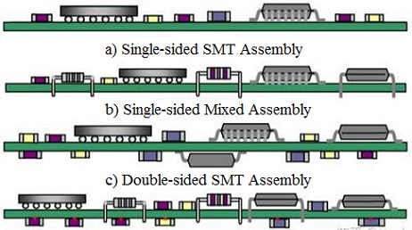
Figure 7: Schematic Diagram of Common Wave Soldering Double-sided Mixed Assembly
According to the number of copper clad layers, PCB can be divided into the following three types:
1) Single-sided board: only one side is routed or covered with copper.
2) Double-sided board: both the top layer and the bottom layer will be wired or covered with copper.
3) Multi-layer board: in addition to the top and bottom layers, the middle also includes signal layers, middle layers, power layers, and ground layers, where each layer is insulated from each other and connected through vias.
Note: Because double-sided PCBs have poor electromagnetic compatibility, they are usually only used in low-speed designs.
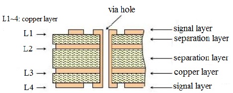
Figure 8: PCB Functional Layers
Each layer of PCB can be connected using through holes, blind holes, or buried holes. In general, most board-level EDA tool software defines the PCB functional hierarchy in the table below.
* 4-Layer PCB Reference Design
|
Ply Sequence
|
Layer 1
|
Layer 2
|
Layer 3
|
Layer 4
|
|
Case 1
|
GND
|
Signal 1+Power
|
Signal 2+Power
|
GND
|
|
Case 2
|
Signal 1
|
GND
|
Power
|
Signal 2
|
|
Case 3
|
GND
|
Signal 1
|
Signal 2
|
Power
|
1) For case 1, an ideal four-layer board stacking design, because the outermost layer is the ground layer, which has a shielding effect on EMI, and at the same time, the power layer and the ground layer can be very close, so that the internal resistance of the power supply is small. However, when the component density is relatively high, the integrity of the ground layer cannot be guaranteed, the signal quality will become poor, and the crosstalk between adjacent signal layers will be large.
2) For case 2, this method is more commonly used. This structure has a better layer capacitance effect, the interlayer crosstalk of the entire PCB is small, and the signal layer can achieve better signal integrity. Since the signal layer is on the surface, the intensity of space electromagnetic radiation increases, and an external shielding shell is required to reduce EMI.
3) For case 3, the power layer and the ground layer are both on the surface layer, and the signal integrity is relatively good. Among them, the signal quality on the signal 1 is the best. This design has a certain shielding effect on EMI, but due to the large loop, the device density directly determines the signal quality, and the adjacent signal layer cannot avoid interlayer interference, which is not as good as the first structure as a whole, unless there are special requirements for power supply.
* 6-Layer PCB Reference Design
|
Ply Sequence
|
Layer 1
|
Layer 2
|
Layer 3
|
Layer 4
|
Layer 5
|
Layer 6
|
|
Case 1
|
Signal 1
|
GND
|
Signal 2
|
Signal 3
|
Power
|
Signal 4
|
|
Case 2
|
Signal 1
|
Signal 2
|
GND
|
Power
|
Signal 3
|
Signal 4
|
|
Case 3
|
Signal 1
|
GND
|
Signal 2
|
Power
|
Signal 3
|
Signal 4
|
|
Case 4
|
GND
|
Signal 1
|
Power
|
GND
|
Signal 2
|
GND
|
1) Case 1 is one of the common methods. The signal layer 1 is a better wiring layer, and the signal layer 2 is the next; but pay attention to the interlayer crosstalk between signal 2 and signal 3. If signal 4 has no components, Just try to reduce the number of signal lines and cover them with an extra layer of grounding.
2) In case 2, the signal integrity of the signal 2 and signal 3 layers is the best. The signal 2 layer is the best wiring layer, and the signal 3 layer is the next. The impedance of the power plane is better, and the interlayer capacitance is larger, which is beneficial to suppress the EMI of the entire board. However, due to the large interlayer interference between signal 1 and signal 2, and far from the distance from the power layer and ground layer, the EMI space radiation intensity is relatively large, and an external shielding shell may be required.
3) Case 3 is the best layout of six-layer pcb. Where signal 1, signal 2, and signal 3 are all good wiring layers, and the impedance of the power plane is also small. The only drawback is signal 4 too far from the ground layer.
4) In case 4, although the performance is better than the previous three cases, the number of layers available for wiring is only 2.
3. Signal Integrity
Signal Integrity (SI) means that the signal on the PCB can still remain complete and correct after being transmitted through the signal line. When the signal in the circuit can be transmitted with the correct timing, the required duration and voltage amplitude to the output end, it means that the circuit has good signal integrity. Obviously, the purpose of it is to ensure the correct transmission of signal timing and voltage amplitude. And the related problems in circuit design mainly focus on the following aspects:
Transmission delay refers to the fact that the signal does not arrive at the receiving end with a certain duration and amplitude within the specified time, usually due to the transmission line effect of driving overload and wiring too long. In addition, the capacitance and inductance on the transmission line will also cause it in the state switching of the signal. In the design of high-speed circuits, it is an unavoidable problem, so a concept of delay tolerance is specially introduced. That is, the maximum timing change of the signal allowed under the premise of ensuring the normal operation of the circuit.
Reflection refers to the echo on the transmission line. Part of the signal power is transmitted from the source to the load through the transmission line, and the other part is reflected to the source. In high-speed circuit design, if the impedance is matched (source impedance, transmission line impedance, and load impedance are equal), reflection will not occur. On the contrary, if not, it will cause signal reflection from the receiving end to the source end. Factors such as the geometry of the wiring, improper termination, transmission through the connector, and discontinuity of the power plane can all cause this problem, resulting in severe overshoot or undershoot of the transmitted signal. And eventually cause the waveform distortion and timing disorder of the signal.
Crosstalk refers to the electromagnetic coupling caused by induced voltages and currents between signal lines that are not electrically connected. This coupling will cause the signal lines to act like antennas. Among them, capacitive coupling will cause coupling current, and inductive coupling will cause coupling voltage, which will increase with the increase of clock speed and reduction of PCB size. All are caused by the magnetic field because of alternating signal current pass through the signal line. Further more, the PCB's working layer, the signal line spacing, the electrical characteristics of the driving and receiving ends, the termination method of the signal line itself, etc. will also have a certain impact on interference.
Ground bounce refers to a large amount of noise generated between the power supply and the ground plane due to a large current surge in the circuit. The instantaneous current, and the parasitic inductance, capacitance, and resistance between the chip package and the power supply will cause power supply noise, resulting in large voltage fluctuations in the circuit at zero potential, which will affect the normal operation of other components.
PCB Design Basic Rules
1. 3W/20H/55 Rules
3W Rule: It means that the center distance between two traces should greater than 3 times the line width, thereby reducing crosstalk between traces. Under this, it can be sure that 70% of the electric fields between the lines will not interfere with each other.
20H Rule: The edges of multi-layer PCBs will radiate electromagnetic interference outwards, make the size of the power supply plane smaller than the size of the ground plane by 20 times the distance between each other, so that the electric field is only conducted within the ground layer, thereby effectively suppressing this edge radiation. And 20H rule can limit 70% of the electric field in the ground plane.
55 Rule: When the clock frequency reaches 5MHz or the rise time of the pulse signal is less than 5ns, the PCB must use a multi-layer board, and sometimes a double-layer board structure is used due to cost considerations. In this case, it is best to use one layer of the PCB as a complete the ground plane layer.
2. PCB Layout Rules
Five Key Points
1) Power supply and signal should be separated.
2) The input and output of signals should be separated.
3) The digital part and the analog part should be separated.
4) The high frequency part and the low frequency part should be separated.
5) The strong current part and the weak current part should be separated.
Basic Principles of Components Layout
1) Under normal conditions, all components should be distributed on the same surface of the PCB. Only to an intensive degree, some patch components with limited height and low heat generation should be placed on the bottom layer.
2) Important unit circuits and core components need to be laid out first, and key signal lines should be kept as short as possible.
3) High voltage and high current signals are completely separated from small current and low voltage signals, analog signals are separated from digital signals, high frequency signals are separated from low frequency signals, and the isolation of high frequency components must be sufficient.
4) Fully refer to the schematic block diagram and place the main components according to the main signal flow direction.
5) The layout of components should facilitate signal flow and keep signals in the same flow direction as possible.
6) Under the premise of ensuring electrical performance, components should be placed on grids arranged parallel or vertically to ensure neatness and beauty.
7) If there is a high potential difference between components or wires, the distance between them should be increased to avoid accidental short circuit caused by discharge breakdown.
8) Components with high voltage should be placed as far as possible in a place that is not easily accessible by hand during debugging.
9) Components located on the edge of the PCB must be at least 2 board thicknesses away from the edge.
10) The same type of plug-in components and polarized components should be placed in the same direction, as much as possible to facilitate later production inspection.
11) Avoid contact between components in different metal packages.
12) The spacing between components needs to meet the requirements of the operating space, such as plugging and unplugging TF cards.
13) Components with heavy weight should be installed close to the PCB support point to reduce the warpage under stress, and cannot be fixed solely by the pin welding surface.
14) Maintain a wide electrical isolation zone between high-voltage components and low-voltage components, that is, do not place components with large voltage levels together, which is beneficial to electrical insulation and can also isolate signals to improve anti-interference capabilities.
Prevent Electromagnetic Interference
1) For components with strong electromagnetic radiation, the distance between them should be increased or a shield should be added, and the direction of component placement should cross the adjacent copper wires.
2) For components that generate magnetic fields such as transformers, speakers, and inductors, attention should be paid to reducing the cutting of printed wires by magnetic force lines during layout, and the magnetic field directions of adjacent components should be perpendicular to each other to reduce the coupling between them.
3) Do not place inductors side by side at close range to avoid mutual inductance.
4) Shield the source of EMI and ensure that the shielding cover is well grounded.
5) For high-frequency circuits, the influence of distribution parameters between components needs to be considered.
Suppress Thermal Interference
1) The heating element is preferentially arranged in a position conducive to heat dissipation, and heat sinks and cooling fans can be installed separately if necessary.
2) Some integrated blocks with large power consumption, large or medium power tubes, resistors and other components should be arranged in places where heat dissipation is easy, and separated from other components by a certain distance.
3) When components are placed on both sides of the PCB, heating components are generally not placed on the bottom layer.
4) Heat-sensitive components such as resistors, capacitors, and crystal oscillators should be kept as far away from high-temperature areas as possible to avoid thermal interference.
5) Thermal devices should be placed at the upwind outlet as much as possible, with tall components placed behind short components and in the direction with the least wind resistance to avoid obstruction of the air duct.
6) Use a large area of grounded copper foil to improve the heat dissipation efficiency of the PCB.
7) The ground mounting holes can use larger pads to make full use of the mounting bolts and the copper foil on both sides of the PCB for heat dissipation.
Power Layout
1) Use more star topology and less daisy chain layout to shorten the public circuit of the power supply.
2) The input and output of the power supply should be laid out separately to avoid crosstalk problems.
3) The power management chip, backlight chip, and boost chip need to be placed in the shielding case.
4) The power supply wiring should be kept away from the radio frequency area as much as possible.
High-speed Components and Antenna Layout
1) Memory chips such as DDR, SDRAM, and NAND Flash need to be placed close to the CPU, and the length of lines and the number of cross lines should be minimized.
2) The screen socket should follow the direction of the CPU outlet, and the RC filter in the middle should be placed on the side of the CPU as much as possible.
3) The high-speed device CPU, LCD screen socket, etc. should be kept away from the antenna module.
4) There should be no metal components around the radio frequency module and the antenna, so as not to affect the frequency point, impedance and other parameters of the antenna.
PCB Wiring Principles
1) The traces of high-speed signals should be as short and straight as possible, the trace spacing should be large enough, and they should be as close to the edge of the PCB or the connector as possible.
2) The line width of the same signal transmission line needs to be consistent, and the same line width needs to be maintained when turning the line.
3) Important signal lines can be increased in width to reduce their characteristic impedance.
4) Key signal lines can be isolated using parallel ground lines.
5) Between two adjacent layers, the wiring should be staggered in a “#” shape.
6) The width of each trace should be symmetrical to the pad connection of each pin of the component, and the line should exit from the center of the component pad.
7) When the trace connected to the pad is wider than the pad, the trace cannot cover the pad and should be led from the end of the pad.
8) The pad pins of chip components with dense pin spacing need to be connected from the outside of the pad, and direct connection to the pads between the pins is not allowed.
9) Vias may cause sudden changes in the impedance of the signal transmission line, so the number of vias needs to be reduced as much as possible.
10) Avoid stubs on the signal transmission line. If it cannot be avoided, the length of the stubs should be less than the rise time of the signal to avoid reflections.
11) When changing layers of high-speed signal wiring, there must be a ground hole nearby to provide a return loop to ensure that the loopback impedance of the entire board is small.
12) Do not use the automatic routing function of EDA tools for analog signals.
13) Use shielded wires for sensitive nodes, for example, add a set of shielded wires with multiple grounding vias around the interfered nodes.
Crosstalk
1) The crosstalk caused by reverse current parallel wiring is large.
2) The crosstalk intensity is directly proportional to the trace length, inversely proportional to the spacing, and directly proportional to the frequency.
3) Increase the spacing between traces, and reduce the parallel length of traces.
4) Adding termination matching can reduce reflections and reduce crosstalk.
5) Limit the signal layer to within 10mil above the ground plane.
6) Insert a ground wire between the two lines with serious crosstalk for isolation, thereby reducing crosstalk.
7) Avoid noise sources, such as MCU, inductors, and crystal oscillators, it is strictly forbidden to route or drill holes on the surface adjacent to the crystal oscillator.
Copper Clad
1) It is best to choose a larger ground plane for coverage in areas without wiring to provide shielding and improve decoupling capabilities.
2) Large areas of copper foil should be avoided as far as possible around heating elements or high-current wiring, because long-term heating will cause copper foil to expand and fall off.
3) If a large area of copper foil must be used around the heating element, it is best to use grid copper cladding to release the surface tension.
4) When the wiring distribution of the same layer is unbalanced or the copper distribution of different layers is asymmetrical, the copper clad design is recommended.
5) If there is a large area on the outermost layer of the PCB without wiring, it is recommended to cover the grid with copper in this area, so that the overall copper foil distribution of the PCB is even.
6) It is recommended that the size of the blank square between the copper grids is about 25milx 25mil.
7) Noise-sensitive circuits need to consider ground shielding, that is, ground wires with a width greater than 50mil or ground holes with a spacing of less than 300mil should be placed around the signal layer.
8) When the isolated copper (especially the surface layer) exceeds 150 mils, grounding vias cannot be drilled, and this area needs to be deleted to avoid forming a suspended antenna.
3. PCB Panelization
PCB panelization refers to the processing method that requires V-cut or stamp holes processing of a single PCB board due to the automatic placement of electronic components. There are three common methods:
1) Same-direction panelization: The simplest method can be realized after tiling and copying the same PCB design.
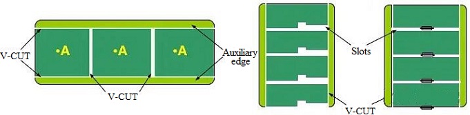
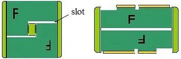
2) Centrally symmetrical panelization: It is suitable for splicing two PCBs with irregular shapes. A slot must be milled in the middle to separate them. If there is a large deformation, you can consider adding auxiliary blocks connected by stamp holes.
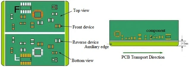
3) Mirror symmetry panelization: It is usually used when the chip components on the front and back of the PCB can meet the reflow soldering requirements. However, it should be noted that it needs to meet the symmetrical distribution of the positive and negative pieces of the PCB light painting. For example, if the second layer of a four-layer PCB is a power/ground negative, the symmetrical third layer must also be a negative, otherwise mirror symmetry cannot be used for imposition.
4. Auxiliary Edge
This is an auxiliary part added to meet the needs of automated patching. It will be removed after production is completed, and is generally 5mm.
1) Positioning hole: Used for positioning during PCB processing and testing, generally a 2mm via hole.
2) Mark point: Used for automatic placement machine identification and positioning, usually designed as a 1mm pad.
5. Test Points
Key components need to add test points to facilitate automated flying probe testing later. The pads used for welding patch components are not allowed to be used as detection points, and dedicated test pads must be designed separately to reduce the impact on solder joint detection and production debugging. Also they need to be distributed on the same side of the PCB as much as possible to reduce inspection time and cost.
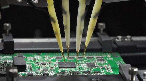
Figure 13: Flying Probe Test
1) The distance between the test point and the edge of the PCB should be greater than 5mm.
2) Ensure that the test points are not covered by solder mask or other ink.
3) The test points are preferably tin-plated or immersed in gold to prevent oxidation.
4) Try to place the test point 1mm away from the component to prevent the component from being mistakenly hit by the probe.
5) The test point needs to be more than 3.2mm away from the positioning hole.
6) The diameter of the test point should not be less than 0.4mm, and the distance between adjacent test points should be more than 2.54mm.
7) Components with a height exceeding 6.4mm cannot be placed on the test surface to avoid the test fixture of the probe hitting these high components.
8) Make sure that each chip has power and ground test points, and as close as possible to the chip (preferably less than 2.54mm).
9) When setting test points on the PCB trace, the width of the test pad can be appropriately enlarged.
10) The test points should be evenly distributed on the PCB to avoid excessive concentration of stress caused by the probe pressing down.
11) The power supply should have test points set up in different areas to facilitate decoupling and fault inquiry.
6. Five Elements of PCB Wiring
1) Plan the circuit partition so that the core components are placed in the center of the entire board, and other important components are also distributed as close to the central axis as possible.
2) The power supply is in the first place. The input and output traces of the power supply should be as thick as possible (the line width should not exceed the component pin pad, or select the loop trace), and the power traces between different copper layers can pass through multiple vias ( 2 ~ 6) to improve the current carrying capacity.
3) Have reasonable grounding treatment for important modules and signal routing.
4) Properly fan out the component pins to keep the wiring clearly.
5) The optimal routing layer usually refers to the layer closest to the complete ground plane.
7. Basic PCB Wiring Strategies
1) First place the packaging positions related to mounting holes, connectors, switches and other structural parts.
2) Based on the X/Y position of the package origin, design the relative X/Y position in the package attributes to achieve precise positioning of package placement.
3) First place the main control IC chips, then place others according to functional modules, and finally place other auxiliary components.
4) The smaller the capacitance of the filter capacitor, the closer it needs to be placed to the pins of the IC chip (very important). On the contrary, if the capacitance is larger, it can be properly placed farther away from the pins.
5) During the wiring process, if the flying wires interfere with the connection relationship of the components, the display of the package value and bit number of the EDA tool can be hidden.

 English










