Silicon Carbide (SiC) is widely used in fields such as electronics, power and energy. As a crystal composed of a stable combination of carbon and silicon elements, with unique physical and chemical properties, it is an ideal material for manufacturing high-efficiency, high-temperature and radiation-resistant devices.
Silicon Carbide (SiC) Basic
SiC Characteristics
Compared with traditional silicon (Si), the band gap of SiC is 3 times that of Si, and the breakdown field strength is eight times that of Si. This allows SiC to withstand higher temperatures, stronger electric fields and more strong radiation environment. In addition, SiC semiconductors also have high carrier mobility and excellent resistance to chemical corrosion, making them useful in high temperature, high pressure, high frequency and high radiation environments.
The main form of SiC in IC chips is the substrate, including power devices, sensors, radio frequency devices and logic devices. In the power field, SiC semiconductors are mainly used in high-voltage, high-temperature, and high-power power electronic equipment, such as inverters, motor drives, solar inverters, power supplies, etc. In the energy field, SiC are mainly used for the conversion and storage of renewable energy such as wind and solar energy, as well as the charging and driving of electric vehicles.
Table 1: Physical & Chemical Properties of SiC
|
Properties
|
Description
|
|
Physical
|
High hardness (3000kg/mm), can cut rubies
|
|
High wear resistance, second only to diamond
|
|
The thermal conductivity exceeds that of metallic copper, 3 times that of Si, and 8 to 10 times that of GaAs.
|
|
High thermal stability, and cannot melt under normal pressure.
|
|
Good heat dissipation performance
|
|
Chemical
|
Very corrosion-resistant, resistant to almost any known corrosive agent at room temperature
|
|
The surface of SiC is easily oxidized to form a thin layer of SiO2, which can prevent further oxidation. When the temperature is higher than 1700C, this oxide film melts and the oxidation reaction occurs rapidly.
|
|
The band gaps of 4H-SiC and 6H-SiC are about 3 times that of Si and 2 times that of GaAs; their breakdown electric field strength is one order of magnitude higher than Si, and the saturated electron drift velocity is 2.5 times that of Si. The band gap ratio of 4H-SiC is wider than 6H-SiC.
|
SiC wafers are single crystal flakes formed by cutting, grinding, polishing, cleaning, etc. As a semiconductor substrate material, silicon carbide wafers can be made into power devices and microwave radio frequency devices through epitaxial growth, device manufacturing and other processes. They are an important basic material for the development of semiconductor industry.
According to different resistivity, silicon carbide wafers can be divided into conductive type and semi-insulated type. Among them, conductive type is mainly used to manufacture high-temperature and high-voltage power devices, with large market size; while semi-insulated type is mainly used in microwave radio frequency devices and other fields. With the accelerated construction of 5G communication networks, market demand has increased significantly.
Table 2: SiC Products
|
Products
|
Applications
|
|
SiC Wafer
|
Conductive type
|
1) As a substrate material for SiC diodes, MOSFETs and other power devices.
2) It is suitable for high temperature, high voltage and other working environments, and can be used in new energy vehicles, photovoltaic power generation, rail transit, smart grids, aerospace and other fields, etc.
|
|
Semi-insulated type
|
1) As a substrate material used for microwave radio frequency devices such as HEMT after epitaxial growth, device manufacturing, and packaging testing.
2) Mainly used in 5G communications, satellites, radar and other fields
|
|
Others
|
Seed crystal
|
A "seed" wafer with the same structure as the desired SiC single crystal, used to produce SiC crystals.
|
|
Specifications
|
It can be used for processing SiC wafers, equipment development and testing, among which semi-insulating silicon carbide crystals can be used to manufacture moissanite and related products.
|
SiC Production
The hardness of SiC is second only to diamond, and it can be used as an abrasive for grinding tools such as grinding wheels. Therefore, uses diamond grinding wheels for processing SiC is a better way. However, SiC material not only has the characteristics of high hardness, but also has high brittleness and low fracture toughness, which makes it easy to cause brittle fracture of the material during the grinding process, leaving them on the material surface, and causing serious surface and semi-subsurface damage. Therefore, in-depth study of SiC grinding mechanism and subsurface damage is of great significance to improve SiC grinding processing efficiency and surface quality.
Next, let’s talk about the polishing of silicon carbide. The main methods are: mechanical polishing, magnetorheological polishing, chemical mechanical polishing (CMP), electrochemical polishing (ECMP), catalyst-assisted polishing or catalytic-assisted etching (CACP/CARE), friction chemical polishing (TCP, also known as abrasive-free polishing) and plasma-assisted polishing (PAP), etc.
CMP technology is an important means of current semiconductor processing. It is also the most effective process method that can process the surface of single crystal silicon to atomic level smoothness. What’s more, it is the only practical method that can simultaneously achieve local and global planarization when processing.
Typical Applications
1. 5G infrastructure - communication power supply

Communication power supply is the energy bank for server and base stations. It provides power for various transmission equipment and ensures the normal operation of the communication system. For example, the high-frequency characteristics of SiC MOSFET make the magnetic unit in the power circuit smaller and lighter, and the overall power supply efficiency is higher. What’s more, the reverse recovery characteristics of it are almost zero, making it suitable for the 3kW unbridstaggered PFC circuit required efficient communication power supply.
2. New energy vehicles - charging pile power module

The rapid development of the new energy vehicle industry has driven the growth in demand for charging columns. For new energy electric vehicles, increasing charging speed and reducing costs are very important. Here the use of silicon carbide devices in charging pile power modules can achieve high efficiency and high power of charging pile power modules, thereby increasing charging speed and reducing charging costs.
3. Extra high voltage - application of flexible transmission DC circuit breakers
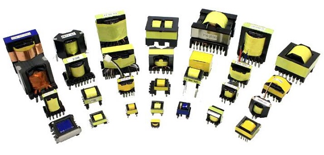
As a large-scale system project, UHV will generate a series of demands for raw materials and components. Power devices are key components of flexible transmission technology in UHV DC at the transmission end and power electronic transformers (PET) at the substation. As one of the key parts of flexible DC transmission, the reliability of DC circuit breaker has a great impact on the stability of the entire transmission system. Here using high-voltage SiC devices in DC circuit breakers can greatly reduce the number of series sub-units, which is a key direction of industry research.
4. Rail transit - traction converters, power electronic transformers, auxiliary converters, auxiliary power supplies

Future rail transit will place higher requirements on power electronic devices, such as traction converters, power electronic voltage converters, etc. The use of SiC power devices can greatly improve the power density and working efficiency of these devices, which will help significantly reduce the load-bearing system of rail transit. Because SiC devices can achieve further high efficiency and miniaturization of equipment, and have huge technical advantages in rail transportation. Japan's Shinkansen N700S has taken the lead in using silicon carbide power devices in traction converters, significantly reducing the weight of the vehicle, achieving higher carrying efficiency, and reducing operating costs.
Pros and Cons of SiC Products
SiC products are an advanced material widely used in high temperature, high voltage and high frequency environments. Its characteristics are as follows:
Advantage:
1) Excellent high-temperature performance: The melting point of silicon carbide products is as high as 2700°C, which can maintain its structural stability and strength in high-temperature environments. Therefore, it is widely used in high-temperature molten metal, heating furnaces, petrochemical and other fields.
2) Strong corrosion resistance: Silicon carbide has excellent corrosion resistance and can work stably for a long time in acid, alkali and oxidizing environments.
3) High hardness and strength: Silicon carbide has higher hardness and strength than traditional ceramic materials, so it has good wear resistance and impact resistance.
4) Excellent thermal conductivity and electrical conductivity: So silicon carbide is widely used in the manufacturing of high-power electronic components and radiators.
Disadvantages:
1) Expensive: Because of the complex process, the relative SiC products are more expensive.
2) Difficulty in manufacturing: SiC products are difficult to manufacture and require complex production conditions such as high temperature and high pressure.
3) Fragile: SiC products are fragile and are not suitable for environments with larger particles and easy wear.
4) Poor processability: So it is difficult to manufacture SiC products with complex shapes.
Developing Problems
Although SiC power devices have broad application prospects, they are currently limited by factors such as high prices. So far, the market size is not large and the application range is limited. It is mainly concentrated in photovoltaics, power supplies and other fields. The main problems existing in the current applications are:
1) The driving technology of silicon carbide power devices has a long way to go. In order to give full play to the high-frequency and high-temperature characteristics of it, the driver chips are required to have the characteristics of high operating temperature, large driving current and high reliability. At present, they still use the traditional way, which cannot meet the requirements.
2) Also the protection technology is not yet perfect. Silicon carbide power devices have the characteristics of fast switching frequency and short short-circuit time, however, current device protection technology cannot meet the demand.
3) The circuit application switching model of silicon carbide devices cannot fully reflect the switching characteristics of silicon carbide power devices, and cannot provide accurate guidance for the circuit topology simulation design of silicon carbide devices.
4) The electromagnetic compatibility problem in the application of silicon carbide power devices has not yet been completely solved.
5) The circuit topology for silicon carbide power devices is not optimized enough. At present, no new circuit topology has been developed that fully takes advantage of silicon carbide power devices.
Development and Competition
1. SiC Products
1) Single crystal materials of SiC
They mainly include conductive substrates and semi-insulating substrates. High-quality and large size are the primary problems to be solved, further more, continuously increasing wafer size and reducing defect density (micropipes, dislocations, stacking faults, etc.) are its key development directions.
Problems in the development process:
(1) Compared with advanced silicon power semiconductor devices, the size of single crystal substrates is still small and the degree of defects is still high.
(2) The wire cutting process of silicon carbide single crystal substrate material has shortcomings such as large material loss and low efficiency.
(3) The research and development of P-type substrate technology lags behind. At present, the silicon carbide P-type single crystal substrate has high defects and high resistivity. That is, its basic scientific issues have not yet been solved.
2) SiC epitaxial materials
Since silicon carbide devices must be made on epitaxial materials, all silicon carbide single crystal materials will be used generally as substrate materials for growing epitaxial materials. Different from the traditional manufacturing process, SiC power devices cannot be directly manufactured on the related single crystal materials, thereby additional high-quality epitaxial materials must be grown on conductive single crystal substrates and manufactured on the epitaxial layer. And the main epitaxial technology is chemical vapor deposition (CVD).
As the manufacturing requirements and voltage levels of silicon carbide power devices continue to improve, their epitaxial materials continue to develop in the direction of low defects and thick epitaxy. In recent years, the quality of thin SiC epitaxial materials (below 20μm) has been continuously improved.
Problems in the development process:
(1) N-type silicon carbide epitaxial growth technology needs to be further improved.
(2) P-type silicon carbide epitaxial growth technology is still immature. High-voltage silicon carbide power devices are bipolar devices, which put forward requirements for P-type heavily doped epitaxial materials. Currently, there is no low-defect, heavily doped P-type epitaxial material that meets the demand.
3) SiC power devices
SiC power devices include diodes and transistors, of which diodes mainly include junction barrier Schottky power diodes (JBS), PiN power diodes and merged PiN Schottky diodes (MPS); transistors mainly include MOSFET, BJT, JFET, IGBT and GTO, etc.
Problems in the development process:
(1) Silicon carbide single crystal and epitaxial technology are not perfect enough, which makes it very difficult to manufacture high-voltage SiC devices. In addition, the defect density of the epitaxial layer restricts the development of silicon carbide power devices in the direction of large capacity.
(2) The technological level of silicon carbide devices is still relatively low, which is a technical bottleneck that restricts the development and promotion of silicon carbide power devices, especially high-temperature and large-dose high-energy ion implantation processes, ultra-high temperature annealing processes, deep groove etching processes and high-temperature ion implantation processes. In addition, the quality oxide layer growth process is not ideal yet, low reliability under high temperature and long-term operating conditions is obvious.
(3) In terms of reliability verification of silicon carbide power devices, the test standards and evaluation methods still follow silicon devices. In other words, there are no specialized test standards and evaluation methods for SiC power devices, resulting in a gap between test conditions and actual use.
(4) In terms of silicon carbide power device testing, silicon carbide device testing equipment, testing methods and testing standards basically follow the traditional testing methods, resulting in insufficient accuracy of test results such as dynamic characteristics and safe working areas evaluation standard.
4) Silicon carbide power module
In order to further increase the current capacity of silicon carbide power devices, multiple chips are usually integrated and packaged in parallel using module packaging. Because silicon carbide power modules first developed from hybrid power module products composed of silicon IGBT chips and SiC JBS diode chips.
At present, silicon carbide power modules mainly include wire bonding type and flat package type. In order to give full play to the high-temperature and high-frequency advantages of silicon carbide power devices, it is necessary to continuously reduce the parasitic inductance of the power module, reduce the thermal resistance of the interconnection layer, and improve the stable operation ability of the chip at high temperatures.
The main problems currently are:
(1) Using multi-chip parallel silicon carbide power modules, due to small junction capacitance and high switching speed, extremely high current rise rate (di/dt) and voltage rise rate (dv/dt) will occur during the switching process. In this case, serious electromagnetic interference and additional losses will occur, and the excellent performance of SiC devices cannot be exerted.
(2) The packaging process and packaging materials of silicon carbide power modules basically follow the mature technology of silicon power modules. There is insufficient innovation in welding, leads, substrates, heat dissipation, etc. The power modules have large stray parameters and low reliability.
(3) The development of silicon carbide power high-temperature packaging technology lags behind. At present, the technology and materials for high-temperature and high-power-density packaging of SiC devices are not yet fully mature. In order to take advantage of the high-temperature devices, advanced sintering materials and processes must be further developed to achieve overall breakthroughs in high-temperature, high-reliability packaging materials and interconnection technologies.
2. Market Competition Pattern
From the perspective of industrial structure, the current global SiC industry structure is dominated by the United States, Europe, and Japan. Among them, the U.S is at first place in the world, accounting for 70% to 80% of global SiC production and more than 60% of the SiC wafer market; Europe has a complete SiC substrate, epitaxy, device and application industry chain; Japan is the absolute leader in equipment and module development.
Most of the new models that mainstream car companies will release in 2024 and 2025 will use silicon carbide. SiC power devices have been used in key power systems inside new energy vehicles, including traction inverters, DC/DC converters, on-board chargers, etc. According to predictions by relevant agencies, there will be a significant shortage of SiC production capacity. For example, the IGBT shortage may reach its peak in the second half of this year, and the SiC shortage will reach its peak from 2024 to 2025.

 English










