What is the function of a filter in a circuit? In some signal circuits, there are usually some unwanted noises, such as high-frequency noises. At this time, filters are needed to deal with them.
Type of Filter Circuits
There mainly include: capacitor filter circuit, RC filter circuit, LC filter circuit, electronic filter circuit.
1. Characteristics
As shown in Figure 1(a). It is a unidirectional pulsating DC voltage waveform. It can be seen from the figure that the directionality of the voltage is consistent at all times, but it fluctuates in the voltage amplitude, that is, on the time axis, the voltage changes periodically.
According to the rule of waveform decomposition, this voltage can be decomposed into a DC voltage and a group of AC voltages with different frequencies. In Figure 1(b), the dotted line is the DC component of unidirectional pulsating DC voltage U0, and the solid line is the AC component of U0.
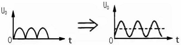
Figure 1: Decomposition of Unidirectional Pulsating Line Voltage
2. Filter Capacitor Principle
According to the above analysis, due to the U0 can be decomposed into two parts: AC and DC. In the filter circuit of the power supply circuit, the AC component in the voltage can be filtered out according to the characteristics of DC blocking and energy storage of the capacitor, or "AC blocking" of the inductor. Figure 2 shows the schematic diagram of the filter capacitor.
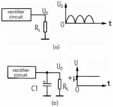
Figure 2: Filter Capacitor Schematic Diagram
Figure 2(a) is the output circuit of the rectifier circuit. After the AC voltage is passed through the rectifier circuit, the output is unidirectional pulsating direct current, which is U0.
Figure 2(b) is a filter capacitor circuit. Since the capacitor C1 is equivalent to an open circuit to the DC, the DC voltage output by the rectifier circuit cannot pass through C1 to the ground, and can only be added to the load RL. The figure is RL. For the AC component output, because C1 has a large capacity and small capacitive reactance, the AC component flows to the ground through C1 and cannot be added to the load RL. In this way, through the filtering of the capacitor C1, the required DC voltage +U is extracted from the unidirectional pulsating DC.
The larger the capacity of the filter capacitor C1, the smaller the capacitive reactance to the AC component, so that the smaller the AC component remaining on the load RL, the better the filtering effect.
3. Principle of Inductor Filter
Figure 3 shows the schematic diagram of the inductor filter. Since the inductor L1 is equivalent to a path to the DC, the DC voltage output by the rectifier circuit is directly added to the load RL.
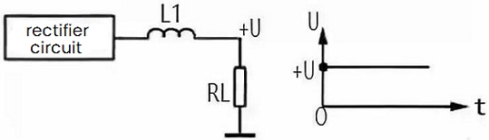
Figure 3: Filter Inductor Schematic Diagram
For the AC component output by the rectifier circuit, because L1 has a large inductance and inductive reactance, it has a great effect on the AC component, preventing the AC from flowing through C1 to the load RL. In this way, through the filtering of the inductor L1, the required DC voltage +U is extracted from the unidirectional pulsating DC.
The greater the inductance of the inductor L1, the greater the inductive reactance to the AC component, so that the smaller the AC component remaining on the load RL, the better the filtering effect, but the DC resistance will also increase.
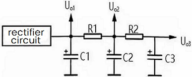
Figure 4: RC Filter Circuit (π-type)
* Circuit Principles
(1) The filtering principle of this circuit is: the voltage output from the rectifier circuit is first filtered by C1 to filter out most of the AC components, and then added to the filter circuit composed of R1 and C2. The capacitive reactance of C2 and R1 form a voltage divider circuit. Because the capacitive reactance of C2 is very small, the attenuation of the divided voltage of the AC component is large, and the purpose of filtering is achieved. For direct current, since C2 has a direct blocking effect, the voltage divider circuit of R1 and C2 does not have the effect of partial voltage attenuation on direct current, so that the direct current voltage is output through R1.
(2) When the size of R1 remains unchanged, increasing the capacity of C2 can improve the filtering effect, and when the capacity of C2 remains unchanged, increasing the resistance value of R1 can improve the filtering effect. However, the resistance value of the filter resistor R1 should not be too large, because the DC current flowing through the load will flow through R1, and a DC voltage drop will be generated on R1, which will reduce the DC output voltage Uo2. The greater the resistance of R1, or the greater the current flowing through the load, the greater the voltage drop across R1, resulting in a lower DC output voltage.
(3) C1 is the first capacitor filter, increasing the capacity can improve the filter effect. However, when C1 is too large, it will take a long time to charge C1 when starting up, and this charging current flows through the rectifier diode, and it will be damaged when the charging current is too large and the time is too long. Therefore, the use of this RC filter circuit can make the capacity of C1 smaller, but the filtering effect can be further improved by rationally designing the values of R1 and C2.
(4) There are three DC voltage output terminals in this filter circuit, which respectively output three sets of DC voltages Uo1, Uo2 and Uo3. Among them, Uo1 is only filtered by capacitor C1; Uo2 is filtered by C1, R1 and C2, and the AC component in Uo2 is smaller; Uo3 is filtered by 2 filter circuits, and the filtering effect is the best.
(5) The magnitudes of the three DC output voltages are different. Uo1 has the highest voltage, and it is directly added to the power amplifier circuit, or to a circuit that requires the highest DC operating voltage and the largest operating current; while the voltage of Uo2 is slightly lower, because the resistor R1 has a voltage drop to the DC voltage; and the voltage of Uo3 is the lowest, this voltage is generally supplied to the pre-stage circuit as a DC working voltage, providing low working voltage and less AC component.
4. LC Filter Circuits ( π-type)
Figure 5 shows the LC filter circuit. It is basically the same as the π-type RC filter circuit. This circuit just replaces the resistor with a inductor, because it has the same resistance to DC and AC, and the inductor has a large inductance to AC and a small resistance to DC, which can improve the filtering effect without reducing DC output voltage.
In Figure 5, the unidirectional pulsating DC voltage output by the rectifier circuit is first filtered by capacitor C1 to remove most of the AC components, and then added to the L1 and C2 filter circuits. For the AC component, L1 has a large inductive reactance, so the AC voltage drop on L1 is large, and it is small to the load.
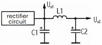
Figure 5: LC Filter Circuit (π-type)
For direct current, since L1 does not present inductive reactance, it is equivalent to a path. At the same time, the diameter of the inductor lead is relatively thick, and the DC resistance is small, so there is basically no voltage drop, resulting in the direct current output voltage is relatively high, which is the main advantage of using inductor filter circuit.
Electronic Filter Diagram Recognition Methods
1. Electronic Filter
Figure 6 shows it. VT1 in the circuit is a triode, which acts as a filter tube, C1 is the base capacitor filter of VT1, R1 is the base bias resistor of VT1, RL is the load of this filter circuit, and C2 is the capacitor filter of the output voltage.
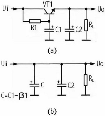
Figure 6: Electronic Filter Circuit
The working principle of the electronic filter circuit is as follows:
(1) VT1, R1, and C1 in the circuit form an electronic filter circuit. This circuit is equivalent to a capacitor with a capacity of C1×β1. Where β1 is the current magnification of VT1, and it is relatively large, so the equivalent capacitance is large, which shows good filtering performance of the electronic filter.
The equivalent circuit is shown in Fig. 6(b), where C in the figure is the equivalent capacitance.
(2) R1 and C1 in the circuit form an RC filter circuit. On the one hand, R1 provides base bias current for VT1 and is also a filter resistor. Since the current flowing through R1 is the base bias current of VT1, this current is very small, and the resistance value of R1 can be relatively large, so that the filtering effect of R1 and C1 is very well, and the AC component is minimal. Because the emitter voltage has the characteristic of following the base voltage, the AC component in the VT1 emitter output voltage is also very small, which achieves the purpose of filtering.
(3) In electronic filters, filtering is mainly realized by R1 and C1, which is also an RC filter circuit, but it is different from the RC filter circuit introduced earlier. In this circuit, the DC current flowing through the load is the emitter current of VT1, and the current flowing through the filter resistor R1 is the base current of VT1. The base current is very small, so the resistance value of the filter resistor R1 can be set very large ( good filtering effect), but it will not drop the DC output voltage much.
(4) The resistance value of R1 in the circuit determines the base current of VT1, then the tube voltage drop between the collector and emitter of VT1, and finally the output DC voltage of VT1 emitter. So change the value of R1, you can adjust the DC output voltage +V.
2. Electronic Voltage Stabilization Filter
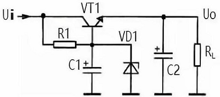
Figure 7: Electronic Voltage Regulator Circuit
Figure 7 shows another electronic voltage stabilizing filter. Compared with the previous circuit, the voltage stabilizing diode VD1 is connected between the base of VT1 and the ground. The principle of electronic voltage regulation is as follows:
After the Zener diode VD1 is connected between the base of VT1 and the ground, the input voltage passes through R1 to make VD1 in a reverse biased state. At this time, the voltage characteristics of VD1 stabilize the base voltage of the VT1 tube, and the DC voltage output by VT1 emitter is also relatively stable.
R1 is also a current limiting protection resistor for VD1. After adding VD1, changing the value of R1 can not change the VT1 emitter output voltage. Because there is a PN junction voltage drop at the emitter of VT1, the emitter output voltage is slightly smaller than the regulated value of VD1.
C1, R1 and VT1 form an electronic filter circuit.
In some occasions, in order to further improve the filtering effect, a double-tube circuit can be used, that is, two electronic filter tubes constitute a composite tube circuit. In this way, the total current magnification is the product of the current magnifications of each tube, which obviously can improve the filtering effect.
* Summary
The following points should be paid attention to in the analysis of power filter circuit:
(1) When analyzing the working principle of the capacitor filter, it is mainly to use the "DC blocking" feature of the capacitor, or the characteristic of charge & discharge, that is, to charge the filter capacitor when the rectifier circuit outputs a unidirectional pulsating DC voltage. If not, the filter capacitor discharges the load.
(2) When analyzing the working principle of the inductor filter, it is mainly to understand that the inductor has a small resistance to DC and has no inductive reactance, but for AC has.
(3) When analyzing the electronic filter circuit, it is necessary to know that the capacitor on the base of the electronic filter tube is the key component of the filter. In addition, to analyze the DC circuit, the electronic filter tube has base current, collector and emitter current, and the current flowing through the load is the emitter current of the electronic filter tube. Changing the base current can adjust the collector of the electronic filter tube voltage drop between the emitter and the emitter, thus changing the DC voltage output by the electronic filter.
(4) The output DC voltage can be stabilized after adding a Zener diode.
Cutoff Frequency Calculation
The formula for the cutoff frequency of the first-order RC filter is: f=1/(2πRC)
Such as R=51Ω, C=22uF, then the cut-off frequency f=141Hz. This means that the high-pass RC filter will suppress signals below 141Hz, while the low-pass filter will suppress signals above 141Hz. (In actual use, a margin should be left. Because when the cutoff frequency is reached, the signal has already experienced 3dB attenuation. Generally, the selected cutoff frequency value is slightly larger than the highest frequency of the actual useful).
* Filter Impedance Matching
Using the above method, you can easily design an RC filter, but you will find that the same frequency can have many values, such as R=51Ω, C=22uF, or you can change it to R=510Ω, C=2.2uF. What differences are there? After building the actual circuit, you will find that the output waveform and the input waveform have different amplitudes, why? This involves the problem of filter impedance matching, that is, the filter itself also has impedance, which will divide the signal and reduce the output signal.
Taking the above low-pass filter as an example, assuming that the output impedance of the previous stage circuit is Ro1, and the input impedance of the subsequent stage circuit is RL2, then the equivalent circuit diagram made:
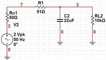
Figure 8: Low-pass Filter Equivalent Circuit
First consider the input impedance of the low-pass filter, the equivalent diagram is simplified as:
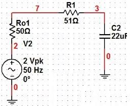
Figure 9: The Equivalent Circuit
Filter input impedance:
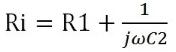
Figure 10: Input Resistance
Then the voltage at Point7 in the figure is:
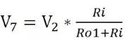
Let's look at the relationship between the output impedance of the filter and the load. The equivalent diagram is:
Where the output voltage of Point 3 in the figure:
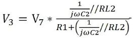
According to the formulas of V7 and V3, the relationship between the input signal and the output signal can be obtained. It can be seen that the selection of the filter R and C values has a great influence on the output of the filter. The selection of R and C parameters is very important.
* So how to choose R and C?
In the case of calculating the cutoff frequency, the values of R and C can be multiplied, such as 51Ω, 22uF becomes 510Ω, 2.2uF or 5.1Ω, 220uF. In order to obtain the waveform with the minimum amplitude attenuation, it is necessary to ensure:
1) The impedance R1+Xc of the filter should greater than the input impedance of the previous stage, the bigger the better.
2) The capacitor impedance Xc of the filter should smaller than the output impedance RL2 of the subsequent stage.

 English










