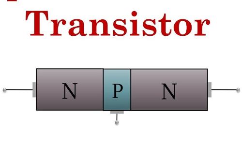
Since the bipolar transistor was the first transistor to be invented, when one simply says "transistors," it sometimes means bipolar transistors. A bipolar junction transistor is a three-terminal semiconductor device that consists of two p-n junctions which are able to amplify or magnify a signal. It is a current controlled device. The three terminals of the BJT are the base, the collector, and the emitter.
What is a Bipolar Transistor?
Bipolar junction transistors (BJTs) are transistors formed by pn junctions. Unlike field effect transistors, which are unipolar, BJTs derive their name from their dual charge carrier operation involving both holes and electrons.
A bipolar junction transistor (BJT) comprises three semiconductor sections that establish two junctions. These transistors come in two configurations: npn and pnp. We provide npn transistors that can handle voltages up to 800 V and pnp variants up to -600 V. Moreover, our range includes built in bias resistor transistors (BRTs). Additionally, we supply radio frequency (RF) transistors designed specifically for low noise amplifier (LNA) and oscillator functions.
The two types of BJT (Bipolar Junction Transistor) transistors are:
Two types of bipolar transistor are available, known as npn and pnp, based on the type of junction.
The structure of a bipolar transistor exhibits symmetry. For instance, in an npn transistor, both the collector and emitter, positioned on either side of the base's p-region, consist of n-regions and appear identical. Yet, the dopant concentrations between the collector and emitter regions differ significantly. As a result, if you reverse the emitter and collector terminals, the transistor's hFE value drops considerably, leading to unintended functionality.
When operating in its active region, a bipolar transistor's collector current is essentially hFE multiplied by the base current. This characteristic allows for the configuration of amplifier circuits in this operational state.
Conversely, in the saturation and cut-off regions, bipolar transistors serve as effective switches. The saturation region exhibits minimal electrical resistance between the emitter and collector, while the cut off region experiences negligible current flow.
NPN Transistor: In this type, the semiconductor material is doped with impurities so that there are two layers of negative (n-type) semiconductor material separated by a layer of positive (p-type) semiconductor material.
PNP Transistor: Here, the semiconductor material is doped such that there are two layers of positive (p-type) semiconductor material separated by a layer of negative (n-type) semiconductor material.
These two configurations allow for different characteristics and applications depending on the specific requirements of a circuit or electronic device.
How do NPN and PNP Transistors Operate?
A bipolar junction transistor (BJT) comprises three distinct regions: collector, base, and emitter. The base, situated thinly between the collector and emitter, hosts two pn junctions. To ensure a significant current gain, the emitter region undergoes much denser doping than the base.
By applying a forward voltage, VBE, between the base and emitter, the BJT activates the PN junction present there. The voltage influences the energy barrier between the base and emitter, governing the emitter current. Due to the emitter's elevated impurity concentration, a substantial carrier flow ensues, and minimal recombination occurs in the slender base. This setup effectively amplifies the base current.
Consider an npn transistor where the collector potential surpasses the emitter's, and the base potential lies approximately 0.7 V above the emitter's. Here, the base emitter junction is forward biased, while the base-collector junction remains reverse-biased. In this biasing, a minute current flows into the base, introducing holes into its p-doped region. This initiates a lowered energy barrier between the base and emitter, prompting electrons from the emitter to diffuse towards the base. Given the disparity in impurity concentrations and the base's slimness, the majority of electrons transition to the collector, constituting the collector current.
The DC current gain, hFE, largely hinges on the variance in impurity concentration between the base and emitter and the base's thickness. Essentially, a BJT is a device where the collector current is modulated by the base current.
Now, for the pnp transistor scenario: Assume the collector potential is inferior to the emitter's, and the base potential is about 0.7 V beneath the emitter's. In a pnp transistor, electrons enter the n-doped base region. This action reduces the energy barrier, facilitating hole diffusion from the emitter. Some of these holes recombine with the introduced electrons, while the rest traverse the base to the collector.
Why Use Bipolar Junction Transistors?
Bipolar transistors function as current controlled devices, wherein a minimal base current leads to a more substantial current flow between the emitter and collector. Unlike transformers, which amplify either current or voltage, transistors have the capacity to amplify both simultaneously. While a BJT typically amplifies current in its prevalent emitter configuration, its integration into a circuit allows for easy modification to amplify output voltage. Hence, due to their versatility in signal amplification, bipolar transistors find widespread application across various circuits, systems, and products.
Bipolar junction transistors have the capability to amplify both analog and digital signals. Additionally, they can serve as switches in DC power supplies or operate as oscillators. Although BJTs are primarily engineered for current amplification in analog applications, they can also act as electronic switches in digital circuitry.
Function of Bipolar Junction Transistor
Amplification: A primary function of a BJT is to amplify current or voltage signals. When a small current flows into the base-emitter junction, a larger current flows between the collector and emitter. This current amplification forms the basis for many electronic circuits like amplifiers.
Switching: BJTs can act as electronic switches, transitioning between a state of high resistance (OFF state) to low resistance (ON state). When the base-emitter junction is appropriately biased, the BJT conducts, allowing a significant current flow between the collector and emitter. Conversely, when the junction is reverse-biased, minimal current flows, effectively turning the BJT off.
Signal Processing: BJTs are crucial components in various signal processing applications. They can be used in oscillators to generate waveforms, in modulators to change the properties of a signal, and in detectors to extract information from a signal.
Control Element: BJTs serve as control elements in many electronic circuits. By modulating the base current, the collector current (or voltage) can be controlled, allowing for precise regulation and operation of devices like motors, LEDs, and other electronic components.
In essence, the bipolar junction transistor is a versatile semiconductor device that plays a fundamental role in analog and digital electronic circuits due to its amplifying and switching capabilities.
KUKE insists on supplying only original electronic components, such as high quality rf coupler directivity. If you have any question, please contact KUKE immediately.

 English